

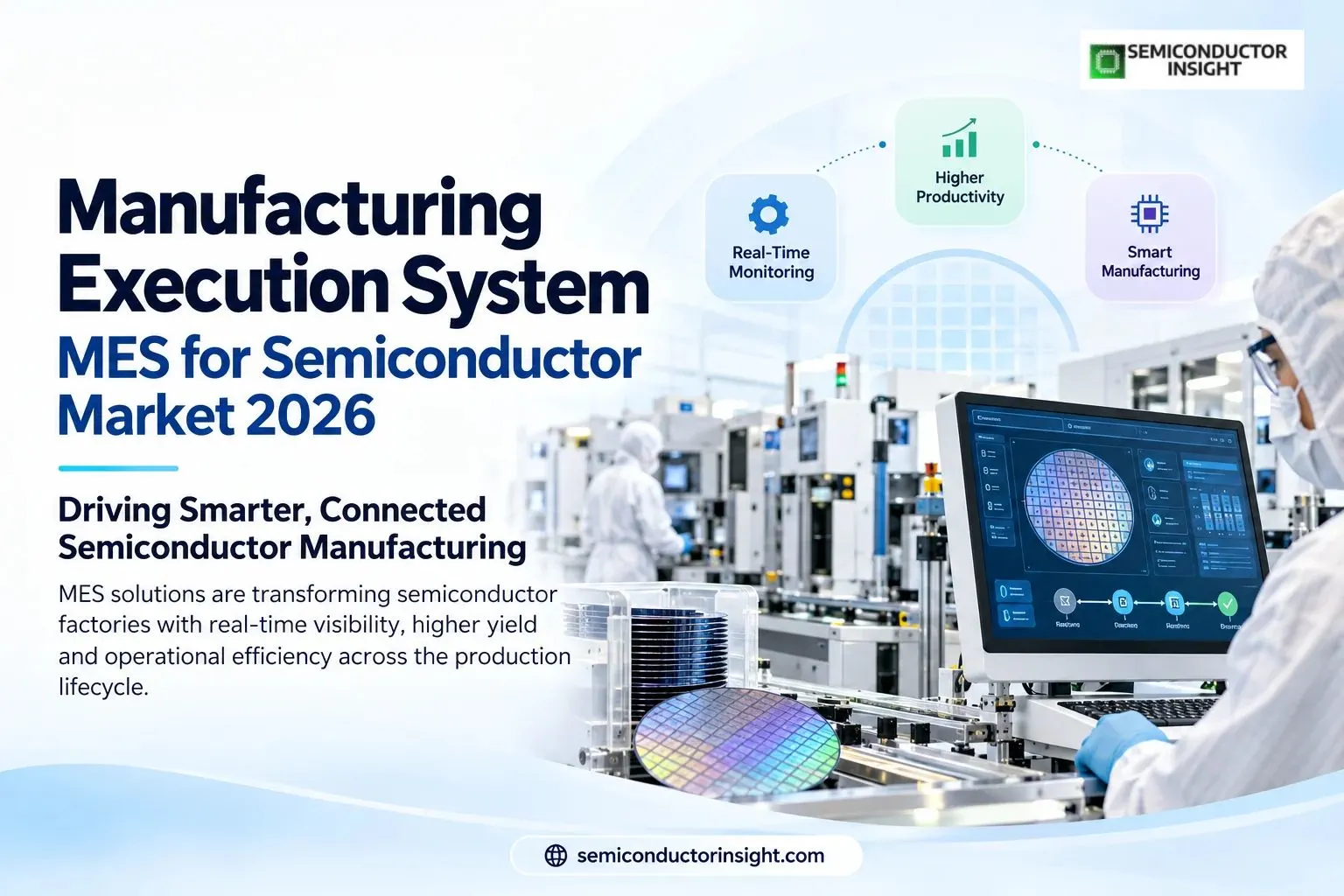
Manufacturing Execution System MES for Semiconductor Market 2026 with Smart Dispatching Recipe Control and Real Time Production Visibility
The semiconductor factory is becoming a software-defined production environment. Every wafer moves through hundreds of tightly controlled operations, while equipment, recipes, inspection systems, material handling and engineering platforms continuously generate data.
Manufacturing Execution Systems, or MES, are increasingly becoming the operational layer that connects these activities and turns factory data into controlled production decisions. SEMI identifies customized MES, AI and machine learning, industrial IoT, digital twins and production analytics as important components of the emerging Smart Fab model.
More Fabs Means More Digital Execution
- The scale of upcoming semiconductor manufacturing expansion is creating a strong requirement for software that can coordinate increasingly complicated production environments.
- SEMI’s Smart Manufacturing Initiative states that more than 100 new and expanded wafer fabs are expected to begin volume production by 2027. The organization also has more than 120 member companies participating in its Smart Manufacturing Initiative.
- For MES providers, this creates an opportunity that extends beyond installing production-management software. New fabs require connected systems from the beginning, making digital execution part of factory architecture rather than an afterthought.
The Semiconductor MES Workflow Is Becoming Intelligent
The traditional MES role was centered on production tracking, work-in-progress management and process control. Modern semiconductor platforms increasingly connect these functions with equipment automation, recipe management, quality systems and analytics.
- Wafer enters fab → MES assigns route → Equipment executes process → Sensors generate data → Inspection validates result → MES updates genealogy → Analytics identifies deviation → Production rules adjust next action
Siemens’ semiconductor-specific MES architecture, for example, includes real-time dispatching, recipe management, wafer genealogy, quality management and equipment connectivity.
Wafer Genealogy Is Moving Into the Spotlight
Traceability is particularly important as semiconductor manufacturing becomes more complex. A wafer can pass through numerous process stages before becoming individual dies, making it difficult to identify the precise manufacturing history behind a defect without granular production records.
Modern semiconductor MES platforms can maintain single-wafer genealogy and connect process information with inspection and production records. This supports faster investigation when yield abnormalities appear and allows manufacturers to trace process conditions throughout the wafer lifecycle.
TSMC Shows Where Intelligent Manufacturing Is Going
- TSMC provides a useful real-world example of this transition.
- The company reports annual manufacturing capacity exceeding 17 million 12-inch-equivalent wafers across its facilities and subsidiaries.
- Its manufacturing strategy increasingly incorporates intelligent operations and advanced process-control technologies.
- TSMC also describes an intelligent manufacturing environment combining MES with Advanced Process Control and Automated Material Handling Systems.
- Its advanced packaging operations incorporate AI, machine learning, big-data analysis and edge computing alongside these systems. tsmc.com
For More Detailed Insights, You Can Surf Our Latest Report Here: https://semiconductorinsight.com/report/manufacturing-execution-system-mes-for-semiconductor-market/
AI Is Turning MES into a Decision Layer
AI is changing the purpose of factory data. Instead of simply recording what happened, connected manufacturing systems can help identify abnormal process behavior, evaluate production conditions and support corrective decisions.
TSMC says its process-control infrastructure incorporates intelligent detection, diagnosis and self-learning, with AI technologies being applied to areas including fault detection and classification and advanced equipment control. TSMC
This creates a new MES architecture:
MES data → AI analytics → anomaly detection → process recommendation → human approval or automated response → updated production data
The result is a gradual move toward closed-loop manufacturing rather than simple production monitoring.
Digital Twins Add a Virtual Factory Layer
- Digital twins are becoming another important extension of semiconductor MES.
- SEMI published a 2026 white paper examining digital twins for AI-driven autonomous semiconductor factories, highlighting their role in modeling and optimizing complex manufacturing environments.
- A digital twin can allow manufacturers to test production scenarios virtually before changing live operations.
- Siemens similarly describes combining semiconductor MES with production simulation and digital-twin capabilities to evaluate bottlenecks, dispatching rules and equipment utilization. Siemens
2026 Signals a Shift from MES Software to Fab Intelligence
SEMI reported in July 2026 that global 300mm fab-equipment spending is expected to exceed $150 billion in 2027 for the first time, supported by AI-chip demand, advanced-capacity investment and supply-chain resilience initiatives. SEMI
As fabs become larger, more automated and more geographically distributed, MES is increasingly positioned as the connective layer between engineering, equipment, materials, quality and production. The opportunity is therefore shifting from basic manufacturing tracking toward intelligent execution, real-time traceability, AI-assisted decisions and increasingly autonomous semiconductor factories.

Comments (0)