
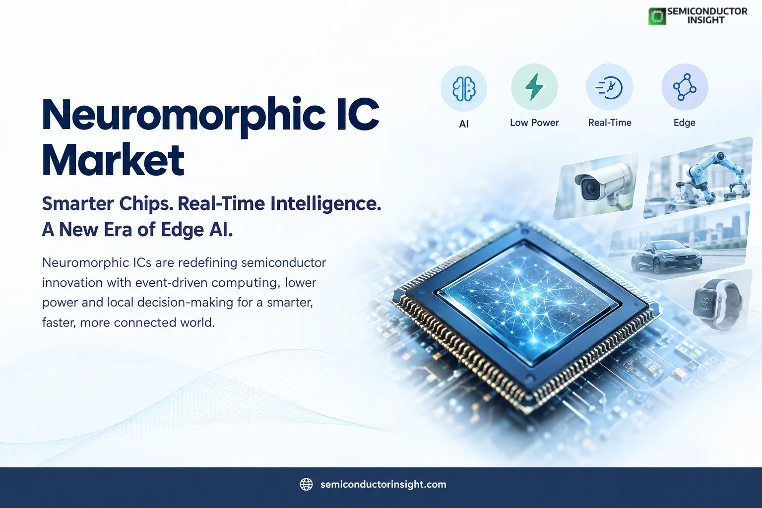
Loihi 2 and Hala Point 2026 Update: How Neuromorphic IC Market Development Is Advancing Edge AI?
Neuromorphic IC Market is developing around a different semiconductor philosophy from conventional CPUs and GPUs. Instead of continuously moving large blocks of data between processing and memory, neuromorphic architectures attempt to imitate elements of biological neural systems through event-driven computation, sparse communication and localized memory.
That distinction is becoming increasingly relevant as AI moves from cloud infrastructure toward cameras, robots, vehicles, industrial machines and other devices that need to react locally.
The Architecture Is Changing the Conversation
Neuromorphic chips are designed around spiking neural networks, where information can be represented through the timing and occurrence of electrical events rather than continuous streams of conventional numerical operations. This allows hardware to remain relatively inactive when useful information is not arriving.
Intel’s Loihi 2 provides a useful reference point. Fabricated on Intel 4, the research processor contains 2.3 billion transistors, up to 128 neuromorphic cores, as many as 1 million neurons and up to 120 million synapses on a chip. Intel also reports that Loihi 2 can provide up to 10 times the processing capability of its predecessor.
Hala Point Changes the Scale
- The technology becomes more striking when individual ICs are connected into a larger neuromorphic system.
- Intel’s Hala Point system contains 1,152 Loihi 2 processors, supporting up to 1.15 billion neurons and 128 billion synapses distributed across 140,544 neuromorphic processing cores. The system occupies six rack units and has a maximum power consumption of 2,600 watts.
- That scale demonstrates an important direction for neuromorphic hardware: researchers are no longer testing the concept only with small experimental chips.
- Large systems are being assembled to investigate practical workloads involving AI, scientific computing and real-time processing.
Data Movement Is Becoming the Real Hardware Problem
One of the strongest reasons neuromorphic architecture is attracting semiconductor attention is the cost of moving information. Conventional AI accelerators can spend substantial energy transferring weights and intermediate data between processing elements and memory.
IBM’s NorthPole provides another example of a memory-centric architectural response. Its 12-nanometer chip contains 22 billion transistors, 256 cores and 192 MB of distributed SRAM, with more than 13 TB/s of on-chip memory bandwidth. IBM reported substantially improved energy efficiency and latency in selected inference workloads compared with conventional processors.
- Neuromorphic IC development takes this concept further by combining local processing, memory and event-based communication around the behavior of neural networks.
Where the Chips Become Interesting
The most compelling applications are those where information arrives continuously but meaningful events are relatively sparse. Cameras, microphones, industrial sensors, robotic systems and wearable devices can therefore become natural environments for neuromorphic processing.
A conventional camera might repeatedly transmit complete frames even when little has changed. An event-based vision system can instead communicate changes occurring at individual pixels. This can reduce unnecessary computation and allow machines to respond to movement with very low latency.
- In January 2026, researchers reported an event-based neuromorphic sensing system integrating a flexible haptic sensor array, event-triggered circuitry and a memristive system-on-chip. The experimental platform achieved 87%–92% recognition accuracy while reducing the energy-delay product compared with conventional digital processing.
For More Detailed Insights, You Can Surf Our Latest Report Here: https://semiconductorinsight.com/report/neuromorphic-ic-market/
Does Tesla Use Silicon Carbide?
Yes, but silicon carbide and neuromorphic ICs belong to different semiconductor application categories. Tesla’s use of SiC is primarily associated with power electronics rather than brain-inspired computing.
The Tesla Model 3 became an important automotive SiC reference after adopting SiC MOSFETs in its traction inverter. Published technical analyses of the inverter identified 24 SiC MOSFETs, while Oak Ridge National Laboratory documentation describes the Model 3 as an early automobile using SiC MOSFETs in its inverter.
The distinction is useful: neuromorphic ICs optimize information processing, while SiC power devices improve high-power electrical conversion. A semiconductor ecosystem can therefore use both technologies for entirely different functions.
The New Edge Computing Equation
The emerging neuromorphic hardware stack can be represented as:
Sensor Event → Spike Generation → Local Neural Processing → Immediate Decision → Minimal Data Transfer
This architecture is particularly relevant when sending every raw sensor signal to a remote processor is inefficient. Robotics, autonomous machines, industrial monitoring and intelligent healthcare devices can potentially benefit from processing information closer to where it is generated.
Why 2026 Matters for Neuromorphic Hardware?
The technology is moving beyond the idea of simply building a “brain-like chip.” Current research is combining spiking neural networks, event-based sensing, in-memory computing, memristive devices and heterogeneous edge systems.
The important semiconductor question is therefore shifting from how many conventional operations a chip can execute to how efficiently it can detect, interpret and react to meaningful events. That change gives neuromorphic ICs a distinct role in the next generation of low-power intelligent electronics, particularly where response time, energy consumption and local decision-making matter more than massive centralized computation.

Comments (0)