
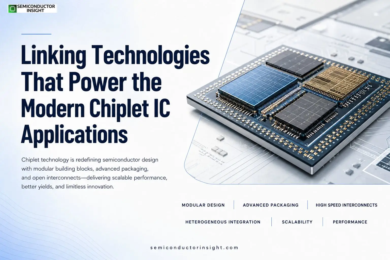
Linking Technologies That Power the Modern Chiplet IC Market Applications
Chiplet technology represents a fundamental shift in how semiconductors are built, moving away from single large monolithic chips toward modular building blocks that combine specialized functions. Each chiplet handles a specific task, such as processing, memory, or input/output, then interconnects with others through advanced packaging to create powerful, flexible systems. This approach helps overcome physical and economic limits of traditional designs, allowing manufacturers to mix dies from different process nodes for better yields and customization.
- Early concepts for chiplets appeared in research projects around the mid-2000s, with contributions from academic efforts like those at the University of California, Berkeley. The idea gained traction as companies sought ways to scale performance without exponentially increasing costs or defect risks on massive dies. Today, major implementations power everything from data center processors to AI accelerators, demonstrating real-world scalability.
- One prominent example comes from AMD’s EPYC and Ryzen processors, which use multiple chiplets linked via high-speed fabrics. This design enabled higher core counts while maintaining cost efficiency by producing compute dies on leading nodes and I/O dies on mature processes.
Flow of Chiplet Assembly Process
Individual dies fabricated separately → Tested for quality → Interconnected using bridges, interposers or direct bonding → Packaged into a unified system → Deployed for high-performance computing or specialized applications. This modular path reduces risk compared to one giant chip.
Government initiatives further support adoption. The U.S. CHIPS and Science Act has funded advanced packaging and heterogeneous integration research through programs at NIST, emphasizing chiplets for national security and supply chain resilience. DARPA’s CHIPS program explored modular computers using chiplets to lower barriers for custom designs. These efforts aim to build domestic capabilities in trusted packaging and interconnect standards.
In high-performance computing, chiplets enable systems like NVIDIA’s Grace Hopper superchip, combining CPU and GPU elements for AI workloads. Supercomputers such as Japan’s Fugaku have utilized related multi-die approaches with silicon interposers for exceptional memory bandwidth. These deployments show how chiplets deliver low latency and high throughput essential for scientific simulations and large-scale training models.
Don’t Forget to Surf Our Updated Report for More Detailed Analysis: https://semiconductorinsight.com/report/chiplet-ic-market/
Example Chiplet-Based Systems
Chiplet-based systems are advancing rapidly, with several leading platforms already showing how modular design improves performance across different computing environments. AMD EPYC uses multiple compute chiplets combined with I/O to deliver higher core counts and better manufacturing yields, making it well suited for servers and data centers. Intel OCI Chiplet integrates optical I/O with the CPU to support high-bandwidth AI interconnects in data center infrastructure, while NVIDIA Grace Hopper combines CPU and GPU chiplets to accelerate AI processing for supercomputing and model training.
Standards organizations are also playing an important role in this transition. The Universal Chiplet Interconnect Express, or UCIe, consortium is promoting open interfaces so chiplets from different vendors can work together more smoothly, much like standardized building blocks in other industries. This approach reduces reliance on a single supplier and helps speed up innovation across the ecosystem.
Adapted Integration Spotlight: Which Processor Platforms Integrate Best With AI Accelerator Ecosystems?
- Leading solutions from AMD and Intel stand out for their mature ecosystems. AMD’s Infinity Fabric allows efficient chiplet-to-chiplet communication ideal for scalable server farms.
- Intel’s Foveros and EMIB packaging technologies support tight integration of diverse functions, including optical interfaces for next-generation AI data movement.
- These platforms excel in environments requiring massive parallel processing while maintaining power efficiency and thermal performance. Developers often prefer them for hybrid setups combining general computing with specialized accelerators.
- Ongoing global scenarios reflect broader adoption. European and Asian initiatives complement U.S. efforts, focusing on automotive and edge computing where chiplets offer customization for sensors and power management.
- In data centers handling exploding AI demands, chiplet-based designs help manage heat and energy while scaling performance.
- Recent demonstrations at industry events showcased live optical chiplet operations, highlighting readiness for deployment in hyperscale facilities.
- The versatility of chiplets extends to custom silicon projects. Smaller teams or specialized applications benefit from combining pre-verified modules rather than designing everything from scratch.
- This lowers development time and cost, opening opportunities in fields like autonomous systems or advanced telecommunications. Packaging technologies such as 2.5D interposers and 3D stacking further enhance density and speed.
As implementations multiply, the focus remains on reliability through rigorous testing of individual chiplets before integration. Real deployments in trusted environments underscore the technology’s maturity for mission-critical uses.
From supercomputers pushing scientific boundaries to everyday servers powering cloud services, chiplet architectures deliver measurable gains in flexibility and performance. This modular paradigm continues influencing semiconductor design strategies across the globe, supporting sustained innovation in an increasingly connected world.

Comments (0)