
Light Sources for Lithography Market 2026 Technology Breakthroughs
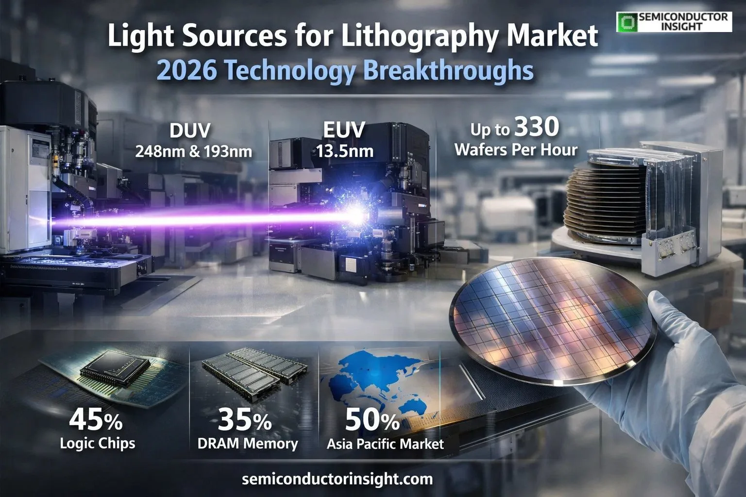
Every advanced semiconductor begins with an extremely precise light beam. Light Sources for Lithography Market forms the backbone of chip fabrication, enabling manufacturers to print billions of transistors onto silicon wafers with nanometer-level accuracy. These light sources operate across wavelengths such as deep ultraviolet (DUV) at 248nm and 193nm, and extreme ultraviolet (EUV) at 13.5nm, each defining how small and efficient chips can become.
Modern fabs process hundreds of wafers per hour, with each wafer containing thousands of chips depending on design complexity. This makes light source efficiency not just a technical parameter, but a direct determinant of production scale and cost efficiency.
From Deep Ultraviolet to Extreme Precision
The transition from DUV to EUV marks one of the most significant technological shifts in semiconductor history. While DUV systems still dominate mature nodes, EUV is rapidly gaining ground, accounting for over 30% of new lithography tool installations in recent years.
EUV light sources enable fewer patterning steps, reducing process complexity while improving accuracy. This is crucial for chips below 7nm, where even atomic-level variations can affect performance. Meanwhile, DUV continues to support advanced packaging and legacy nodes, ensuring a hybrid ecosystem rather than a complete replacement.
Major Key Insights:
· The 1:1 scanner-to-source limit is a hidden cost driver in the industry because each ASML scanner has its own CO₂ laser and tin droplet setup. xLight’s FEL hub-and-spoke approach (one source : 20 scanners) is a structurally disruptive idea. That’s why the US government gave it its first Trump-era award, the $150 million CHIPS Act LOI in December 2025.
· Stochastic defect data from ASML’s own 2024 resist exposures (177 defects/wafer at 32nm pitch, >0.25/cm²) is the kind of process-yield detail that rarely appears outside SPIE lithography conferences it’s why Intel elected not to employ direct EUV exposure for 30nm pitch.
· The FEL vs. LPP comparison isn’t in many market surveys yet because xLight hasn’t made any money yet. However, the difference in physics (no plasma conversion step, customizable wavelength down to ~2nm, and a claim of a 30-year lifetime) is the most believable long-term challenge to ASML’s light source monopoly.
Where Performance Meets Physics
At the heart of EUV systems lies an incredibly complex process: lasers firing at microscopic tiny droplets to generate plasma that emits EUV light. Recent breakthroughs show these systems can target 100,000 droplets per second, highlighting the extreme precision involved in modern lithography.
New-generation systems are being designed to process up to 330 wafers per hour, representing a major leap in throughput and manufacturing efficiency.
This level of engineering pushes the boundaries of optics, plasma physics, and materials science, making lithography light sources one of the most sophisticated technologies ever developed.
Market Structure Reflecting Semiconductor Demand
· Light Sources for Lithography Market is like the semiconductor ecosystem as a whole. Light sources alone make up more than 40% of the parts in EUV lithography systems, showing how important they are to the total system design.
· Logic chips make up around 45% of the market, followed by DRAM at about 35%. This is because there is a lot of demand for high-performance computing and memory-intensive applications.
· Asia Pacific is the most active region, accounting for about half of all activity. This is due to big semiconductor production centres and strong government-backed programs.
Real-World Momentum and Industry Shifts
Recent industry developments highlight how quickly this market is evolving. Leading chipmakers are aggressively scaling EUV adoption for 3nm and upcoming sub-3nm nodes, while governments are increasing investments in domestic semiconductor ecosystems.
In parallel, innovation is not limited to power scaling. Research is exploring alternative plasma methods, compact EUV systems, and even accelerator-based light sources capable of delivering multi-kilowatt output levels, pointing toward the next phase of lithography evolution.
Another emerging trend is the focus on uptime and reliability, with systems now targeting over 90% operational availability, a critical benchmark for high-volume manufacturing.
Lastly, for more in-depth information, don’t forget to read our most recent exclusive report: https://semiconductorinsight.com/report/light-sources-for-lithography-market/
Precision as the New Competitive Advantage
As semiconductor scaling approaches physical limits, the importance of light precision, source stability, and throughput efficiency continues to grow. Light Sources for Lithography Market is no longer just a component segment it is a defining factor in determining which companies can lead the next generation of chip innovation.
From AI processors to advanced memory and automotive electronics, every breakthrough increasingly depends on how effectively light can be controlled at the smallest scales.
In this landscape, the race is not just about smaller nodes it is about mastering the science of light itself.

Comments (0)