Key Statistics
Key Takeaways
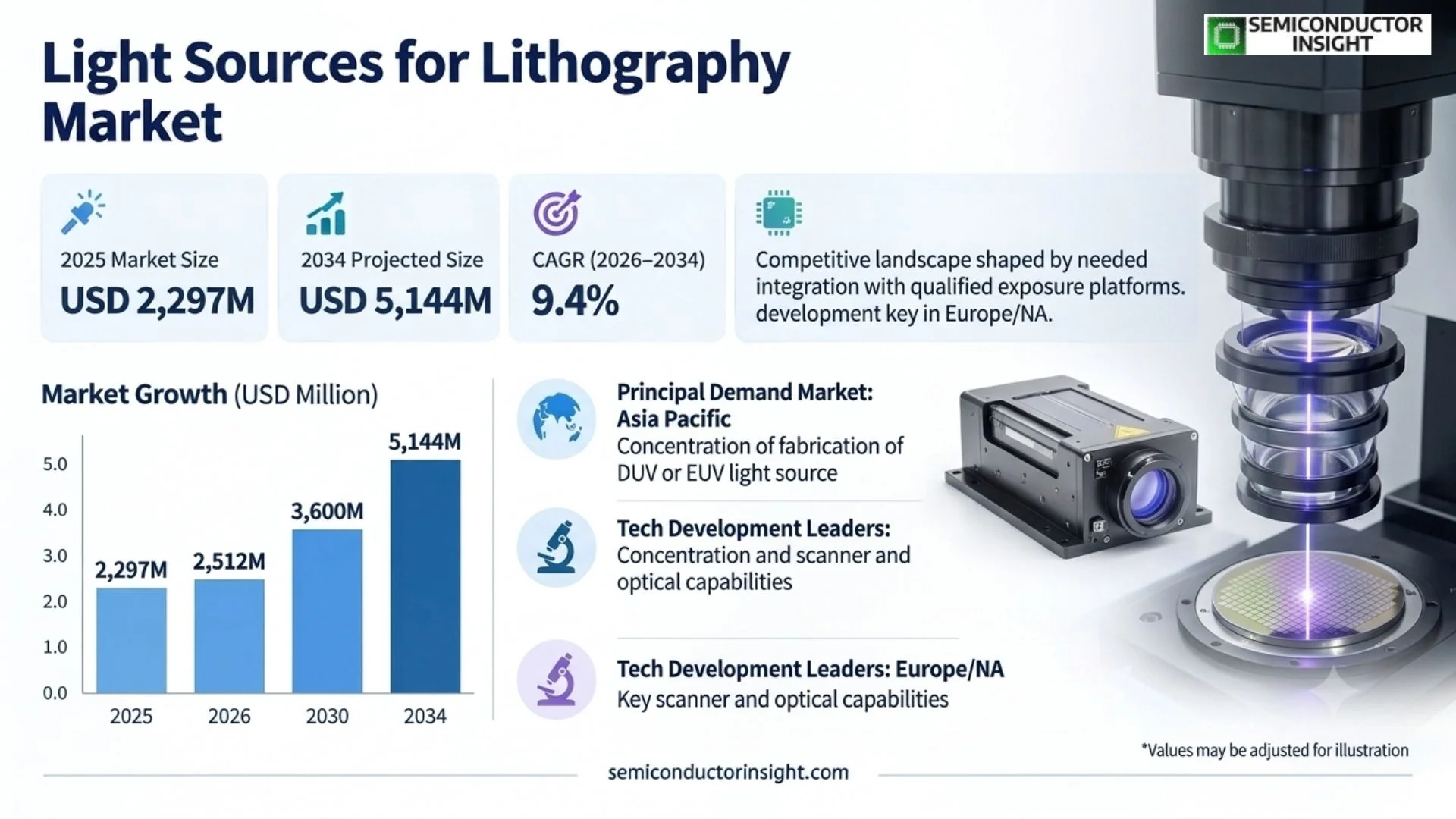
- The global Light Sources for Lithography market is estimated at USD 2,297 million in 2025 and USD 2,512 million in 2026, and is projected to reach USD 5,144 million by 2034, with a CAGR of 9.4% during 2026–2034.
- Light-source performance must be assessed with the exposure system. Usable dose, stability and availability influence wafer output more directly than a standalone peak-power figure.
- DUV and EUV serve different layers and process requirements. EUV adoption does not eliminate the installed base or ongoing need for mature-node exposure technologies.
- ASML reported 48 EUV and 279 DUV lithography systems in 2025. These are scanner figures that provide demand context, not a count or valuation of separately sold light sources.
- The supply chain is highly specialised. Source integration, optical components, maintenance and field support create barriers beyond the ability to generate the required wavelength.
Light Sources for Lithography Market Overview
Light Sources for Lithography Market is estimated at USD 2,297 million in 2025 and USD 2,512 million in 2026, and is projected to reach USD 5,144 million by 2034, with a CAGR of 9.4% during 2026–2034. Asia Pacific is the principal demand market because exposure capacity is concentrated in its semiconductor manufacturing ecosystem; European and North American suppliers remain central to technology development.
Lithography light sources generate the radiation used to transfer patterns during semiconductor manufacturing. The exposure process requires controlled wavelength, dose and stability within a larger system of optics, masks, stages and materials. A source is therefore not equivalent to a complete scanner. Its commercial value is linked to productive wafer exposure and dependable integration with the customer’s qualified manufacturing flow.
ArF and KrF excimer sources support established ultraviolet exposure processes, while EUV uses a different generation and optical architecture. Legacy i-line lamps remain relevant to selected applications even though their wavelength is technically near-ultraviolet rather than deep ultraviolet. These technologies coexist because different layers and devices require different combinations of resolution, throughput and cost. Market demand follows the actual exposure mix used in production.
Segment Analysis: By Type
DUV Light Sources, EUV Light Sources and Others cover distinct exposure technologies. The DUV and legacy ultraviolet category includes ArF, KrF and legacy i-line products, although i-line is technically a near-ultraviolet wavelength. Customers select a source through the requirements of the exposure platform and process. Resolution capability is important, but dose stability, uptime and service economics also determine the commercial value of the installation.
| Type | Demand characteristics |
|---|---|
| DUV Light Sources | ArF excimer lasers at 193 nm and KrF at 248 nm serve established exposure platforms. Legacy exposure products also include 365 nm i-line mercury lamps for legacy and specialised applications. |
| EUV Light Sources | EUV exposure uses 13.5 nm radiation within a vacuum-compatible optical system. Source availability and usable dose are important to productive wafer throughput. |
| Others | Specialised exposure sources support narrower applications and development requirements outside the principal DUV and EUV categories. |
Segment Analysis: By Technology Node
| Technology Node | Commercial relevance |
|---|---|
| Above 28nm | Mature processes prioritise suitable resolution, operating cost and continued support for established exposure equipment. |
| 10-28nm | Layer mix and patterning strategy determine the required combination of exposure technologies. |
| Below 10nm | Demanding patterning requirements increase the importance of advanced exposure and integration, without assigning the same technology to every layer. |
Segment Analysis: By Power Output
| Power Output | Commercial relevance |
|---|---|
| Low Power (Below 50W) | Specialised and lower-output applications require assessment at the specified measurement location and operating conditions. |
| Medium Power (50-100W) | Intermediate output bands should be compared only for compatible source technologies and measurement definitions. |
| High Power (Above 100W) | Higher output can support throughput when the scanner, optics and resist process can use the available radiation effectively. |
Segment Analysis: By Application
Integrated Device Manufacturers, Foundry and Others describe the customer operating model rather than a particular semiconductor product. Both logic and memory manufacturing can require a mix of exposure technologies. Equipment purchases follow process roadmaps, factory capacity and qualified layer requirements. Suppliers need to coordinate with the scanner ecosystem and the customer’s production schedule, because source performance is assessed within a complete manufacturing process.
| Application | Demand characteristics |
|---|---|
| Integrated Device Manufacturers (IDM) | Manufacturers coordinate device roadmaps and fabrication processes, linking source requirements to internal qualification and capacity planning. |
| Foundry | Foundries need exposure capability that supports customer process offerings, layer requirements and dependable factory output. |
| Others | Research and specialised manufacturing users evaluate sources for defined development or production tasks. |
Regional Analysis
Asia Pacific leads demand because of its concentration of wafer fabrication, while Europe controls important scanner and optical integration capabilities. North America combines source engineering with advanced process development and new factory investment. South America has a much smaller direct exposure-equipment footprint, and the Middle East and Africa are primarily downstream demand and selected manufacturing markets. Supplier headquarters, source production and installed exposure capacity must be assessed separately.
Why does lithography demand geography differ from supplier geography?
| Region | Position | Growth outlook | Demand profile | Access gate |
|---|---|---|---|---|
| Asia Pacific | Largest demand | Fab-led | Foundry and memory | Scanner qualification |
| Europe | Technology centre | Roadmap-led | Systems and optics | Integration expertise |
| North America | R&D and manufacturing | Qualification-led | Advanced processes | System integration |
| South America | Small direct market | Selective projects | Specialty and downstream | Service economics |
| Middle East & Africa | Selective direct demand | Project-dependent | Research and computing | Fab infrastructure |
Competitive Landscape
Competition in lithography sources is shaped by the need to integrate with a qualified exposure platform. Generating radiation at the required wavelength is only one part of the task. Customers need stable dose, availability and support within the scanner’s operating requirements. This creates strong engineering relationships and makes substitution difficult when a source change affects the performance of a production process.
Cymer within ASML and Gigaphoton are important participants in the source ecosystem, while USHIO and other specialists address particular exposure applications. Product scope differs across EUV, excimer and legacy lamp technologies. Companies should therefore be compared within the relevant architecture. Scanner market position should not be converted into an unsupported percentage share of the separate light-source market.
The source is embedded in a wider network of optics, lasers, controls and maintenance capabilities. Suppliers that coordinate these interfaces can support improvements in availability and useful output. Field-service execution is particularly important because exposure interruptions can affect factory productivity. Commercial differentiation consequently includes installed-base support and component longevity as well as new-source performance.
Supplier roles and competitive positioning
| Participant group | Positioning |
|---|---|
| Integrated source and scanner ecosystem | Cymer (ASML) operates within an integrated lithography system environment, with source performance linked to platform requirements. |
| Excimer and specialised source suppliers | Gigaphoton and other relevant suppliers compete through ultraviolet source capability and support for compatible exposure systems. |
| Legacy and specialised exposure | USHIO, Beijing RSLaser Opto-Electronics Technology and Optosystems cover different product and geographic niches; offerings are not interchangeable across all lithography technologies. |
Production Capacity Analysis
Source production capacity depends on specialised components, integration expertise and calibration rather than general assembly space alone. Optical quality, laser subsystems, controls and service parts must meet demanding operating requirements. A completed source also needs acceptance within the exposure platform. Capacity analysis should therefore distinguish source manufacturing, scanner shipments and productive installed wafer capacity, which measure different stages of the commercial chain.
ASML’s 2025 mix of EUV and DUV systems illustrates demand across multiple exposure architectures, but those scanner counts are not source shipments. Suppliers also support operating tools through maintenance and replacement components. This creates a capacity requirement that extends beyond new installations. Effective planning must balance product development, manufacturing and field-service resources across a technically diverse installed base.
Market Dynamics
The market combines advanced-node requirements with a large continuing need for established exposure technologies. EUV development increases the importance of source power and availability, while mature processes prioritise dependable operation and cost. Customer investment is cyclical and tied to factory qualification. Suppliers that improve useful exposure output and service economics can create value across both new systems and existing production fleets.
Market Drivers
| Factor | Directional influence |
|---|---|
| Advanced patterning requirements | High positive |
| Productive wafer throughput | High positive |
| Installed-base maintenance | Medium positive |
| Diverse semiconductor expansion | Medium positive |
Advanced patterning requirements
Demanding logic and memory processes need exposure capability that can resolve the required patterns within an economical production flow. Source technology contributes to that capability but must work with optics, masks and materials. Suppliers benefit when their improvements support qualified process performance. The commercial trigger is adoption in a manufacturing layer or platform, rather than the announcement of a smaller node name alone.
Productive wafer throughput
Factories need to expose wafers at useful speed while maintaining the required pattern quality. More usable source power can help when the rest of the platform can exploit it, but stability and availability are equally important. Suppliers that improve the complete operating result can create economic value for customers. This links source demand to factory productivity rather than a standalone wattage target.
Installed-base maintenance
Operating exposure tools require continued support, replacement components and controlled maintenance to preserve performance. This creates a recurring commercial relationship after the initial system installation. Source vendors need reliable service logistics and technical expertise near customer factories. The opportunity depends on the installed platform and operating intensity, offering a different demand pattern from the more cyclical purchase of new equipment.
Diverse semiconductor expansion
New capacity in power, analogue, memory and logic devices does not require one uniform exposure solution. Different processes use different wavelengths and layer strategies. Suppliers can address this diversity with appropriate source technologies and support for established platforms. The market implication is continued coexistence of exposure categories, rather than a simple replacement cycle in which every new factory adopts the most advanced source.
Market Restraints
| Factor | Directional influence |
|---|---|
| Integration complexity | High negative |
| Specialised supply concentration | High negative |
| Capital-spending cycles | Medium negative |
Integration complexity
A source change can affect dose, optics, thermal behaviour and process control across the exposure system. Customers and platform suppliers must evaluate these interactions before introducing a revised product into manufacturing. This creates long development and acceptance cycles. A promising source demonstration therefore does not immediately translate into commercial deployment, particularly when the change requires broader platform or process modifications.
Specialised supply concentration
Critical optical, laser and control components require specialised capabilities and consistent quality. Substituting an alternative supplier can trigger integration and qualification work. This creates concentration risk and limits the speed at which production can expand. Vendors need coordinated supplier development and service-parts planning to protect both new equipment deliveries and the availability of systems already operating in customer factories.
Capital-spending cycles
Exposure-equipment demand follows semiconductor capacity plans that can change with end-market conditions and factory schedules. Source suppliers are exposed to those adjustments through platform production and customer acceptance timing. Installed-base service can provide a different revenue stream, but it does not remove the effect of delayed new systems. Capacity commitments need to reflect both technology readiness and credible customer deployment plans.
Market Opportunities
Availability-focused upgrades
Customers can benefit when a source operates more consistently or requires less disruptive maintenance. Such improvements may increase useful factory output without a complete platform replacement. Suppliers should demonstrate the result under relevant operating conditions and coordinate changes with the scanner owner. The commercial opportunity lies in measurable productivity and service benefits, rather than simply adding a higher peak-power specification.
Energy and consumable efficiency
Exposure sources consume energy and require specialised materials or replacement components. Reducing those operating requirements can improve customer economics when performance is maintained. Vendors need to assess the complete operating cycle rather than a narrow laboratory condition. Improvements that preserve qualified process behaviour can support adoption within existing fleets and strengthen the value of long-term service relationships.
Specialty-device exposure support
Power, analogue and other specialised semiconductor processes need economical and dependable patterning. Suppliers can address these customers through appropriate established technologies, service and replacement support. The opportunity differs from leading-edge EUV development and should be assessed on its own operating requirements. Strong lifecycle support can be commercially valuable where customers intend to run qualified equipment for extended periods.
Collaborative process development
New exposure architectures require coordinated work among source, scanner, optics, resist and manufacturing specialists. Shared development environments can help customers understand the technology before committing to production. Suppliers that participate effectively can shape integration requirements and build qualification experience. The commercial benefit emerges when that knowledge contributes to accepted platforms and repeatable manufacturing, rather than from research participation alone.
Supply Chain Analysis
Materials and optical components
Specialised materials and optical components must tolerate the source’s operating environment while maintaining consistent performance. Quality variation can affect availability and the efficiency of the exposure system. Suppliers need traceable specifications and dependable replacement capability. This stage creates value through reliability and compatibility with the full architecture, not simply through the availability of a nominally equivalent optical part.
Source generation and control
The source combines its generation mechanism with controls that maintain the required radiation output. Different technologies impose different engineering and maintenance demands. Manufacturers must produce consistent behaviour over operating cycles and component lifetimes. Effective control helps the exposure platform deliver the intended dose, making repeatability and integration as important commercially as maximum output measured under favourable conditions.
Scanner integration
The exposure-system manufacturer integrates the source with optics, stages, handling and process controls. This determines how source capability translates into wafer productivity. Changes require careful validation because an improvement in one subsystem may expose a limit elsewhere. Suppliers that understand these interactions can support useful platform advances and avoid treating the source as an isolated commodity component.
Factory service and operation
Installed systems need technical support, maintenance scheduling and spare parts that fit production requirements. Source-related downtime can affect factory throughput, making service execution economically important. Vendors must coordinate with the platform supplier and customer process teams when changes are introduced. A dependable service relationship supports both recurring business and confidence in later equipment purchases or technology upgrades.
Recent Developments
- 2025 operating year
ASML reported full-specification NXE:3800E performance including 220 wafers per hour, with a higher-power source forming part of a broader system upgrade. ASML - 3 June 2024
ASML and imec opened their joint High NA EUV laboratory, supporting early process and ecosystem development. ASML and imec - April 2024
Intel completed assembly of a High NA EUV scanner at its Oregon research site and began calibration, marking a step toward process qualification. Intel
Report Scope & Segmentation
| Attribute | Details |
|---|---|
| Base Year | 2025 |
| Estimated Year | 2026 |
| Forecast Period | 2026–2034 |
| 2025 Market Size | USD 2,297 million |
| 2026 Market Size | USD 2,512 million |
| 2034 Projected Size | USD 5,144 million |
| CAGR (2026–2034) | 9.4% |
| Unit | Revenue in USD million |
| Market boundary | Exposure light-source equipment used in semiconductor lithography, including DUV and EUV systems; excludes complete scanner revenue and non-photonic patterning equipment. |
| By Type | DUV Light Sources; EUV Light Sources; Others |
| By Application | Integrated Device Manufacturers (IDM); Foundry; Others |
| By Technology Node | Above 28nm; 10-28nm; Below 10nm |
| By Power Output | Low Power (Below 50W); Medium Power (50-100W); High Power (Above 100W) |
| By Region | Asia Pacific; Europe; North America; South America; Middle East & Africa |
| Companies and organisations covered | Cymer (ASML); Gigaphoton; Beijing RSLaser Opto-Electronics Technology; Optosystems; USHIO |
Frequently Asked Questions
What is the market size and growth outlook?
The global Light Sources for Lithography market is estimated at USD 2,297 million in 2025 and USD 2,512 million in 2026, and is projected to reach USD 5,144 million by 2034, with a CAGR of 9.4% during 2026–2034.
What is a lithography light source?
It generates the radiation used by an exposure system to transfer semiconductor patterns. The source is one subsystem within a scanner, not the complete exposure tool.
What wavelengths are relevant?
ArF uses 193 nm, KrF uses 248 nm, legacy i-line uses 365 nm, and EUV uses 13.5 nm. Each supports different exposure requirements.
Is i-line technically DUV?
I-line at 365 nm is near-ultraviolet. It is used in legacy exposure systems alongside other ultraviolet technologies.
Will EUV eliminate DUV demand?
No. Different layers and device processes use different exposure technologies. Established ultraviolet platforms remain relevant to mature and specialised manufacturing.
Which region is the main demand market?
Asia Pacific is the principal demand market because of its concentration of wafer fabrication. Supplier headquarters and source-development locations follow a different geographic pattern.
What determines productive source performance?
Usable dose, stability, availability and integration with optics and process controls matter. Peak power alone does not determine wafer throughput.
Can scanner shipments be counted as source shipments?
No. Scanner, source and installed wafer-capacity measures describe different stages of the supply chain and should not be used interchangeably.
Who are the covered suppliers?
The covered companies are Cymer (ASML), Gigaphoton, Beijing RSLaser Opto-Electronics Technology, Optosystems and USHIO, with different technology and application scopes.
What creates recurring revenue?
Maintenance, replacement components and operating support create continuing demand around the installed exposure-tool base, alongside purchases for new systems.
Research Sources & Evidence Base

Get Sample Report PDF for Exclusive Insights
Report Sample Includes
- Table of Contents
- List of Tables & Figures
- Charts, Research Methodology, and more...