
Laser Lens Market and the Next Layer of Semiconductor Processing Precision
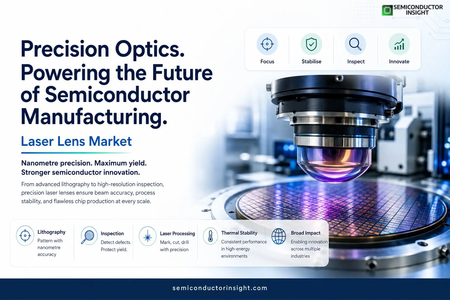
In semiconductor manufacturing, a laser lens is far more than a supporting optical component it directly influences the accuracy of chip production. Every stage involving laser light, from photolithography and wafer inspection to laser marking and micro-processing, depends on precision optics to focus and stabilise the beam.
Modern semiconductor fabs routinely process 300 mm silicon wafers, where a single wafer can contain hundreds to thousands of integrated circuits, depending on chip size. At advanced process nodes below 5 nanometres, even microscopic optical deviations can affect pattern fidelity, making high-performance laser lenses indispensable for maintaining production quality and manufacturing consistency.
Precision Optics Are Driving Every Critical Manufacturing Step
- Laser lenses perform their most valuable role where manufacturing tolerances are measured in nanometres.
- In advanced lithography and optical inspection systems, these lenses must deliver exceptional optical transmission, minimal aberration and excellent thermal stability despite continuous exposure to high-energy laser sources.
- As semiconductor devices become increasingly complex, manufacturers rely on premium optical systems to maintain wafer alignment, improve yield and minimise production defects across millions of chips.
Expanding Laser Technologies Are Supporting Equipment Innovation
The rapid adoption of laser-based manufacturing technologies continues to strengthen demand for advanced optical components. Industry analyses estimate the global semiconductor laser sector at approximately USD 8.45 billion in 2025, increasing to around USD 9.12 billion in 2026, with long-term projections exceeding USD 16 billion over the next decade.
These lasers are widely deployed in wafer processing, optical communication, LiDAR, sensing and industrial automation. As laser performance improves in terms of power, wavelength stability and beam quality, the importance of specialised laser lenses also increases, ensuring efficient beam shaping and consistent optical performance across demanding semiconductor applications.
EUV and DUV Lithography Demand Exceptional Optical Stability
Extreme Ultraviolet (EUV) and Deep Ultraviolet (DUV) lithography represent the most demanding environments for precision optics. EUV systems operate using a wavelength of 13.5 nanometres, while advanced DUV lithography commonly uses 193 nanometre laser sources.
At these dimensions, even minute contamination, thermal expansion or optical distortion can influence feature resolution and critical dimensions on silicon wafers.
Leading-edge lithography tools integrate highly specialised optical assemblies capable of maintaining stable performance throughout continuous manufacturing cycles, supporting the production of advanced processors, memory devices and AI accelerators.
To find out more, feel free to browse our latest updated report: https://semiconductorinsight.com/report/laser-lens-market/
Inspection Systems Are Becoming More Data Intensive
- As semiconductor geometries continue shrinking, defect inspection has evolved into one of the most critical manufacturing processes.
- Modern wafer inspection platforms examine billions of transistor features throughout production using high-resolution optical imaging combined with laser-based metrology.
- Precision laser lenses help detect microscopic particles, alignment variations and surface imperfections that would otherwise reduce manufacturing yield.
- Advanced inspection systems now generate terabytes of process data during routine operations, allowing engineers to identify manufacturing variations earlier and improve overall fabrication efficiency through predictive process control.
How Laser Energy Reaches the Wafer?
Laser Source
│
▼
Beam Conditioning
│
▼
Precision Laser Lens
│
▼
Wafer Exposure or Inspection
│
▼
Pattern Formation and Process Verification
Precision Optics Extend Beyond Semiconductor Manufacturing
- Laser-based semiconductor systems support a broad range of industries including optical fibre communications, automotive LiDAR, consumer electronics, industrial automation, medical imaging, aerospace, defence and scientific research.
- Many of these applications use similar optical architectures, where high-performance laser lenses improve beam quality, focusing accuracy and long-term operational stability.
- As advanced photonics continue expanding across multiple industries, precision optics remain one of the enabling technologies behind next-generation electronic and optical systems.
Precision Keeps This Market Technically Significant
Laser lens market continues to grow in importance because semiconductor manufacturing is becoming increasingly dependent on nanometre-level precision. Every reduction in chip size, every improvement in inspection accuracy and every new generation of lithography equipment raises the performance expectations placed on optical components.
While laser lenses rarely receive the same attention as processors or fabrication tools, they remain one of the critical elements that determine whether advanced semiconductor manufacturing can consistently achieve the precision modern electronics demand.

Comments (0)