
Integrating CMOS THz Detector with On-Chip Patch Antenna Market into Modern Wireless Systems
Engineers have long grappled with the terahertz gap, that tricky slice of the electromagnetic spectrum between microwaves and infrared where conventional electronics falter. CMOS technology, the backbone of everyday chips in smartphones and computers, now steps up with integrated detectors featuring on-chip patch antennas. These compact designs allow direct detection of THz waves right on the silicon die, slashing costs and enabling miniaturization that bulkier systems simply cannot match.
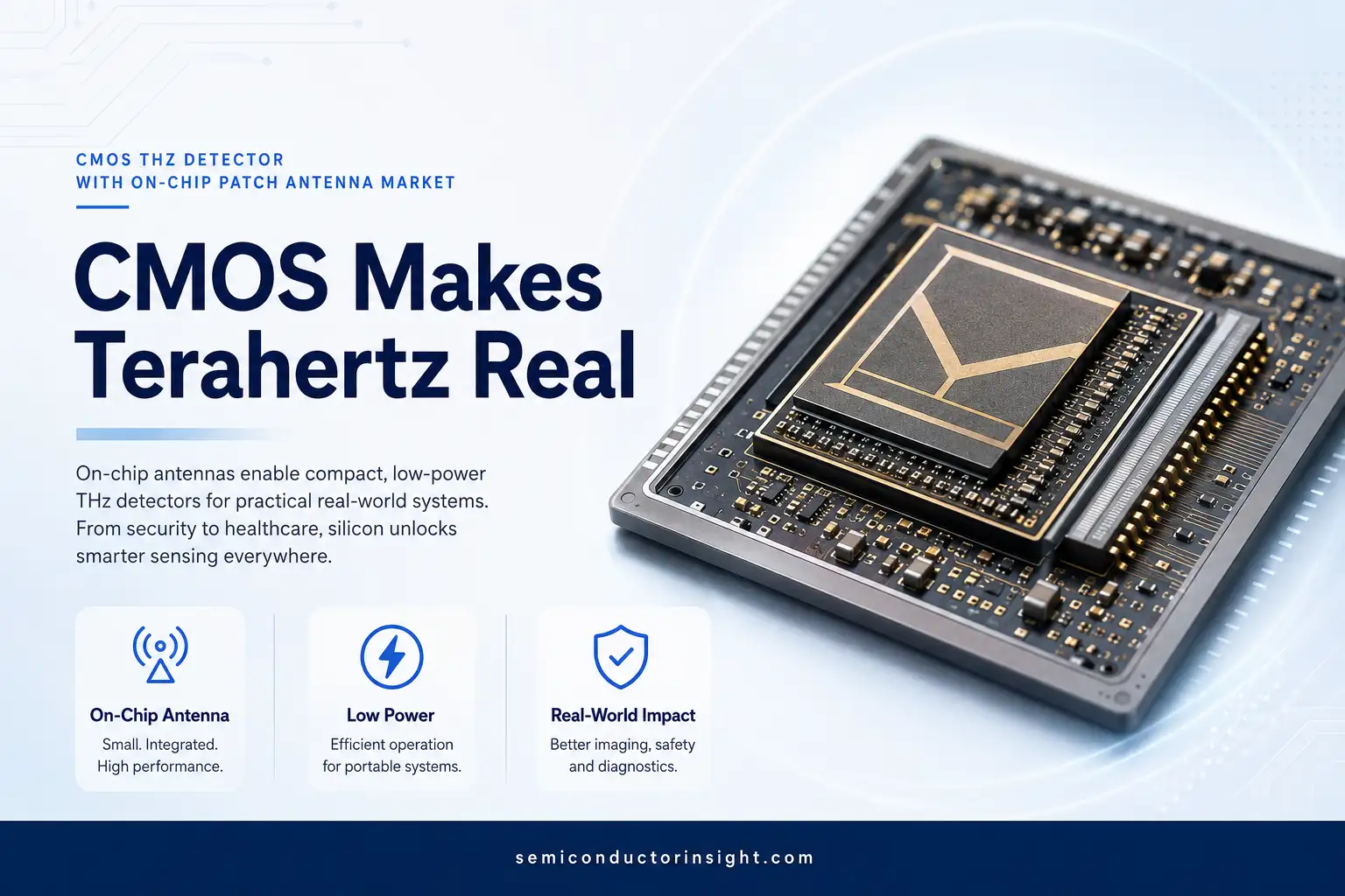
Researchers at various institutions have demonstrated working prototypes in standard CMOS nodes, such as 180nm or 65nm processes, where patch antennas sit atop metal layers to capture signals efficiently. One notable approach uses a V-shaped patch with defected ground structures to boost bandwidth and gain, making the entire detector suitable for array configurations. These on-chip antennas eliminate the need for external bulky components, paving the way for portable THz systems.
Real-World Applications Taking Shape Worldwide
- In security screening, THz waves penetrate clothing and packaging without the ionizing risks of X-rays, revealing concealed items through spectroscopic signatures.
- Airports and high-security facilities explore CMOS-based arrays for real-time imaging, where on-chip integration keeps power draw low enough for continuous operation.
- Medical diagnostics benefit too THz radiation interacts safely with tissue, offering contrast for skin conditions or dental imaging without harmful radiation.
- Early trials at university hospitals combine these detectors with quantum dot enhancements for room-temperature operation, turning standard CMOS cameras into sensitive THz receivers.
- Industrial quality control represents another active area. Manufacturers inspect multilayer composites, pharmaceuticals, and food packaging for defects or contaminants.
- A European research consortium integrated CMOS THz detectors into conveyor-line scanners, achieving resolutions fine enough to spot micron-level voids in plastics.
- In astronomy and atmospheric sensing, similar tech helps map molecular signatures, with compact arrays deployed on ground-based observatories.
Technical Breakthroughs Pushing Performance Boundaries
Recent publications detail detectors reaching sensitivities with noise equivalent power figures in the hundreds of pW per square root Hz range at frequencies around 300-600 GHz. For instance, antenna-coupled MOSFETs in 90nm or 180nm CMOS processes deliver usable response up to 0.75 THz when paired with appropriate lenses or metamaterial absorbers. Patch antennas fabricated in the top metal layers provide directional gain while maintaining compatibility with foundry design rules.
Teams have experimented with asymmetrical FET arrays and annular ring antennas to improve coupling efficiency. One design in TSMC 0.18µm technology targeted 484 GHz operation with a patch fed directly by the detector circuit, demonstrating how monolithic integration reduces parasitic losses. These advances support higher frame rates in imaging arrays, critical for video-rate THz cameras that once required cryogenic cooling.
Supply Chain and Fabrication Dynamics
- Semiconductor fabs increasingly accommodate these specialized structures within standard flows.
- The use of existing copper interconnect layers for antennas and detectors lowers barriers compared to exotic materials like graphene or III-V compounds.
- Government-backed initiatives in the US, Europe, and Asia promote silicon photonics and advanced sensing under broader microelectronics programs, indirectly boosting THz component availability.
- Universities collaborate with foundries to tape out test chips, accelerating iteration cycles from months to weeks.
- Production volumes remain modest but grow as prototypes transition to pilot lines. A single 300mm wafer can yield thousands of detector dies, each incorporating its own patch antenna, supporting cost targets below traditional vacuum-tube or bolometer alternatives for volume applications.
Integration with Emerging Systems
Wireless communications explore THz bands for ultra-high data rates in short-range indoor links. CMOS detectors with on-chip antennas serve as compact receivers in such setups, compatible with 6G research platforms. In automotive radar, extensions beyond 100 GHz leverage similar principles for high-resolution object detection in fog or dust. Defense applications include non-contact threat detection, where portable handheld units benefit from the low-power profile of integrated silicon solutions.
Academic labs publish open-source designs and measurement data, fostering community-driven improvements. One MIT-led effort combined quantum dots with CMOS readout for polarization-sensitive imaging, capturing THz beam rotations at room temperature. Such cross-pollination between photonics and electronics exemplifies the interdisciplinary momentum.
Don’t Forget to Surf Our Updated Report for More Detailed Analysis: https://semiconductorinsight.com/report/cmos-thz-detector-with-on-chip-patch-antenna-market/
Sustainability and Efficiency Angles
Power consumption stands out as a key advantage. Unlike systems needing external amplifiers or cooling, these CMOS implementations operate efficiently at milliwatt levels, aligning with battery-powered or edge-device constraints. Thermal management simplifies too, since on-chip designs dissipate heat locally without complex packaging. As global focus sharpens on energy-efficient electronics, THz detectors that piggyback on mature silicon processes gain favor for their reduced material footprint and recyclability.
Ongoing work optimizes antenna layouts to minimize substrate losses, incorporating techniques like backside etching or substrate lenses for better radiation efficiency. These refinements extend operational lifetimes and broaden deployment scenarios in harsh environments.
Collaborative Ecosystems Driving Progress
- International partnerships between universities, national labs, and industry players accelerate knowledge sharing. Conferences and joint publications highlight measurement setups using homodyne techniques with CMOS TeraFETs, achieving nanoscale resolution in scanning near-field microscopy. Shared fabrication runs under multi-project wafer services democratize access, allowing smaller teams to experiment with custom antenna geometries.
- In Asia, strong semiconductor manufacturing bases support rapid prototyping. North American efforts emphasize system-level integration, while European groups focus on standardization for industrial uptake. This distributed innovation network ensures steady advancements tailored to diverse needs, from scientific instruments to consumer-adjacent tools.
The path forward for CMOS THz detectors with on-chip patch antennas looks promising as fabrication matures and applications multiply. By leveraging proven silicon infrastructure, these technologies stand to make terahertz capabilities routine rather than exotic, opening doors across safety, health, and connectivity domains. Continued refinement in sensitivity, bandwidth, and array scalability will determine how deeply they embed into daily life.

Comments (0)