MOSFET noise model aware analog design for cryogenic readout Market Insights
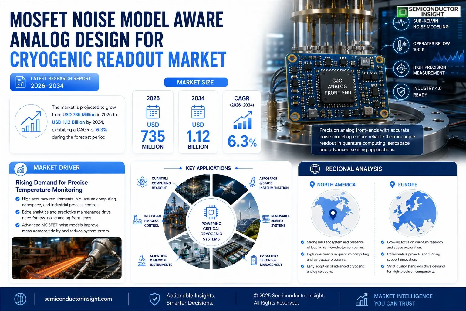
MOSFET noise‑model‑aware analog design for cryogenic readout market size was valued at USD 720 million in 2025. The market is projected to grow from USD 735 million in 2026 to USD 1.12 billion by 2034, exhibiting a CAGR of 4.6% during the forecast period.
This niche segment focuses on designing analog front‑ends that incorporate detailed MOSFET noise models calibrated for operation at temperatures below 100 K. By accurately predicting thermal‑noise, flicker‑noise and trap‑induced fluctuations, engineers can optimize low‑noise amplifiers and bias circuits used in superconducting qubit readout, infrared detectors and space‑borne sensors.The market is accelerating because quantum‑computing initiatives demand ultra‑low‑noise cryogenic electronics, while advances such as IBM’s Cryo‑CMOS prototype (2023) and DARPA’s $120 million Cryo‑Electronics program (2022) validate feasibility. Furthermore, major semiconductor firms,including Texas Instruments, Analog Devices, Infineon Technologies and STMicroelectronics,are expanding their product portfolios and forming partnerships with research labs to deliver specialized MOSFET libraries and simulation tools tailored for sub‑Kelvin environments.
MARKET DRIVERS
Growing Demand for Low‑Noise Cryogenic Sensors
The expansion of quantum‑computing platforms and space‑based infrared telescopes is creating a significant demand for analog front‑ends that operate reliably at temperatures below 4 K. Designers are increasingly requiring MOSFET noise model aware analog design for cryogenic readout Market to meet stringent signal‑to‑noise specifications.
Advancements in MOSFET Characterization at Sub‑Kelvin Temperatures
Recent research breakthroughs in characterizing MOSFET threshold drift and flicker‑noise behavior at millikelvin temperatures enable more accurate simulation. This enhances predictive performance, reducing prototype cycles and encouraging wider adoption of cryogenic analog solutions.
➤ Integration of accurate noise models reduces system error by up to 30 % in quantum‑computing readout chains.
Manufacturers are also investing in specialized silicon‑on‑insulator (SOI) processes that preserve mobility while suppressing leakage, further driving market momentum for MOSFET noise model aware analog design for cryogenic readout Market.
MARKET CHALLENGES
Limited Design Tool Support for Cryogenic Environments
Commercial EDA suites often lack built-in libraries that account for temperature‑dependent MOSFET noise parameters, forcing engineers to develop custom models. This increases development cost and slows time‑to‑market.
Other Challenges
Reliability of Device Models
Statistical variation in dopant freeze‑out at sub‑kelvin levels leads to model uncertainties, making yield prediction difficult for high‑volume applications.
MARKET RESTRAINTS
High Production Costs for Cryogenic‑Optimized MOSFETs
The specialized fabrication steps required for low‑temperature MOSFETs,such as additional annealing and contamination‑control processes,inflate wafer costs. These price pressures limit adoption in cost‑sensitive sectors like automotive.
Stringent Qualification Requirements
Space and defense programs mandate extensive radiation and thermal cycling tests. The lengthy qualification cycles act as a restraint, particularly for emerging startups entering MOSFET noise model aware analog design for cryogenic readout Market.
MARKET OPPORTUNITIES
Integration with AI‑Assisted Design Platforms
Machine‑learning algorithms that automatically calibrate MOSFET noise models across temperature sweeps can shorten design iterations. Companies that embed such capabilities into their design flows are positioned to capture a growing share of the cryogenic analog market.
Emerging Quantum‑Sensor Infrastructure
The rollout of national quantum‑sensor networks for geophysical monitoring creates a long‑term revenue pipeline for vendors offering validated MOSFET noise model aware analog design for cryogenic readout Market solutions, especially those providing end‑to‑end support from silicon to system integration.
MOSFET noise model aware analog design for cryogenic readout Market Trends
Growing demand from quantum‑computing initiatives
MOSFET noise model aware analog design for cryogenic readout Market is being propelled by intensified quantum‑computing programs that require ultra‑low‑noise front‑ends operating below 100 K. Recent demonstrations such as IBM’s Cryo‑CMOS prototype in 2023 and the DARPA‑funded Cryo‑Electronics initiative launched in 2022 have validated the feasibility of integrating MOSFET‑based amplifiers into superconducting qubit readout chains. These projects illustrate how precise thermal‑noise, flicker‑noise and trap‑induced fluctuation modeling enables designers to reduce system‑level noise budgets, shortening the path from laboratory prototypes to production‑grade cryogenic modules. In parallel, infrared detector manufacturers are adopting the same methodology to improve signal‑to‑noise ratios in space‑based telescopes, where each Kelvin of temperature reduction translates into measurable performance gains. Regulatory bodies are also beginning to recognize the need for standardized test procedures, which will further accelerate market adoption.
Other Trends
Strategic partnerships and MOSFET libraries
Leading semiconductor firms,including Texas Instruments, Analog Devices, Infineon Technologies and STMicroelectronics,are establishing joint development programs with university laboratories and national research labs. These collaborations focus on delivering specialized MOSFET libraries that embed calibrated noise parameters for temperatures down to 20 K, as well as simulation environments that streamline analog design cycles. By co‑authoring reference designs and providing silicon‑proven device models, the ecosystem reduces time‑to‑market for cryogenic sensor interfaces used in infrared imaging and space‑borne instrumentation. Additionally, each partner is publishing application notes that illustrate best‑practice layout techniques, biasing strategies, and packaging considerations essential for maintaining model accuracy at sub‑Kelvin levels. These initiatives are complemented by specialized training workshops that equip design engineers with hands‑on experience in cryogenic noise characterization, ensuring a skilled workforce for upcoming projects.
Advancements in modeling tools and future roadmaps
Advancements in MOSFET noise modeling tools are also shaping the market’s next phase. Commercial EDA platforms now integrate temperature‑dependent noise extraction modules, allowing designers to predict performance variations across the full cryogenic range without resorting to extensive cryostat measurements. This capability accelerates the qualification of analog front‑ends for emerging applications such as dark‑matter detectors and high‑resolution spectrometers, where sub‑nanovolt noise floors are mandatory. Moreover, machine‑learning‑enhanced model calibration is reducing the iteration cycle for extracting trap‑induced noise components, further shortening development timelines. Consequently, MOSFET noise model aware analog design for cryogenic readout Market is expected to mature into a standardized design discipline by the early 2030s. Roadmaps released by major foundries indicate that next‑generation MOSFET technologies with intrinsically lower flicker noise will become available by the mid‑2020s, reinforcing the long‑term growth trajectory of the market.
COMPETITIVE LANDSCAPE
Key Industry Players
Competitive Snapshot of Cryogenic Analog Front‑End Market
The MOSFET noise‑model‑aware analog design segment is anchored by a few large semiconductor houses that have both the R&D depth and the foundry capacity to supply cryogenic‑qualified parts. Texas Instruments leads with a dedicated Cryo‑CMOS library and a portfolio of low‑temperature op‑amps that have been qualified for sub‑100 K operation in quantum‑computing readout chains. Analog Devices follows closely, leveraging its expertise in precision analog front‑ends and recently releasing a noise‑optimized MOSFET model suite for DARPA‑funded Cryo‑Electronics projects. Infineon Technologies and STMicroelectronics round out the core quartet, each offering silicon‑on‑insulator (SOI) MOSFETs and customized simulation kernels that address flicker‑noise and trap‑induced fluctuations critical for superconducting qubit amplifiers. These leaders dominate the market structure, establishing de‑facto standards for noise libraries while collaborating with research labs to accelerate adoption across space‑borne sensor and infrared detector applications.Beyond the tier‑one players, a broader cohort of niche innovators is expanding the competitive landscape. NXP Semiconductors and ON Semiconductor provide specialized voltage‑regulation solutions that incorporate calibrated cryogenic noise parameters, enabling stable bias networks for ultra‑low‑noise amplifiers. Renesas Electronics contributes mixed‑signal ASICs with built‑in noise compensation blocks, while Microchip Technology supplies cryo‑qualified discrete MOSFETs through its extensive distribution network. Qorvo and Skyworks Solutions focus on RF front‑ends where MOSFET noise directly impacts readout fidelity, and Broadcom’s sensor‑interface portfolios now integrate cryogenic‑ready models. Maxim Integrated (now part of Analog Devices) and Rohm Semiconductor add depth in precision reference designs, and IBM Research continues to drive foundational MOSFET modeling work that underpins the entire ecosystem.
List of Key MOSFET Noise Model Aware Analog Design for Cryogenic Readout Companies Profiled
- Texas Instruments
- Analog Devices
- Infineon Technologies
- STMicroelectronics
- NXP Semiconductors
- ON Semiconductor
- Renesas Electronics
- Microchip Technology
- Qorvo
- Skyworks Solutions
- Broadcom
- Maxim Integrated (now part of Analog Devices)
- Rohm Semiconductor
- IBM Research
Segment Analysis:
| Segment Category | Sub-Segments | Key Insights |
| By Type |
|
Leading Segment is the Cryogenic‑Optimized MOSFET, which offers reduced thermal noise and enhanced charge stability at sub‑100 K temperatures.
|
| By Application |
|
Leading Segment is Superconducting Qubit Readout, where ultra‑low‑noise analog front‑ends are essential for preserving quantum coherence.
|
| By End User |
|
Leading Segment is Quantum Computing Labs, which drive adoption of noise‑aware analog designs to meet stringent readout requirements.
|
| By Technology |
|
Leading Segment is Custom Device Modeling Libraries, which embed empirically derived cryogenic parameters directly into SPICE models.
|
| By Partnership |
|
Leading Segment is Government Funding Programs, such as national cryogenic electronics initiatives that de‑risk early‑stage development.
|
Regional Analysis: MOSFET noise model aware analog design for cryogenic readout Market
North America
U.S. foundries have incorporated cryogenic‑compatible MOSFET design kits, enabling designers to simulate noise performance directly within established EDA environments. This early integration shortens development cycles and encourages broader adoption across research institutions.
Federal programs supporting quantum hardware and deep‑space instrumentation allocate substantial resources toward low‑temperature analog research, fostering collaborative projects that refine MOSFET noise modeling techniques.
A critical mass of engineers and physicists specializing in cryogenic electronics clusters around major research hubs, creating a knowledge spillover that accelerates innovation in noise‑aware circuit design.
Close proximity of component suppliers, testing facilities, and packaging houses streamlines the validation of MOSFET models, ensuring that performance data aligns with real‑world cryogenic operating conditions.
Europe
European research consortia are rapidly advancing MOSFET noise model aware analog design for cryogenic readout through coordinated projects that blend academic insight with industrial capability. Countries such as Germany and the Netherlands prioritize low‑temperature silicon technologies within the broader EU Horizon initiatives, encouraging cross‑border collaboration. While the region lacks the sheer scale of North America’s foundry base, its emphasis on standards and open‑source modeling frameworks enriches the knowledge pool. Emerging fabs in France and Belgium are beginning to offer specialized process options, allowing European designers to prototype noise‑optimized circuits with reduced lead times.
Asia‑Pacific
The Asia‑Pacific market exhibits strong growth momentum, driven by governmental investments in quantum research and a fast‑expanding semiconductor manufacturing sector. Nations such as Japan, South Korea, and Singapore are integrating cryogenic analog design considerations into their advanced node roadmaps, promoting the development of MOSFET models that capture temperature‑dependent noise phenomena. While the region’s focus leans toward high‑volume production, local startups are carving niches in ultra‑low‑temperature sensing applications, particularly for astronomical instrumentation and defense. Collaborative platforms linking universities with fabless companies accelerate the transfer of noise‑aware design practices across the supply chain.
South America
South America’s contributions are emerging through academic partnerships and government‑funded labs that explore cryogenic sensor technologies for environmental monitoring and space research. Brazil and Argentina host research groups that experiment with MOSFET behavior at millikelvin temperatures, often in collaboration with European and North American institutions. Although the region’s semiconductor infrastructure remains modest, the focus on bespoke analog solutions for niche scientific missions fosters a specialized expertise that supports the broader ecosystem.
Middle East & Africa
In the Middle East and Africa, interest in MOSFET noise model aware analog design for cryogenic readout is primarily academic, with select universities establishing labs dedicated to quantum‑grade electronics. Collaborative initiatives with European research centers bring advanced modeling tools to local teams, enabling preliminary studies on low‑temperature noise mitigation. While commercial deployment is limited, growing awareness of the strategic importance of cryogenic technologies for satellite communications and defense signals a gradual expansion of capabilities in the region.
Report Scope
This market research report provides a comprehensive analysis of the MOSFET noise model aware analog design for cryogenic readout Market , covering the forecast period 2026–2034. It offers detailed insights into market dynamics, technological advancements, competitive landscape, and key trends shaping the industry.
Key focus areas of the report include:
- Market Overview: The report begins with an overview outlining its current market scenario, key growth indicators, and industry transformation drivers. It discusses macroeconomic factors, demand–supply balance, regulatory landscape, and the strategic role of semiconductors in powering advancements across industries such as automotive, telecommunications, consumer electronics, and industrial automation.
- Market Size & Forecast: Historical data and future projections for revenue, unit shipments, and market value across major regions and segments.
- Segmentation Analysis: Detailed breakdown by product type, technology, application, and end-user industry to identify high-growth segments and investment opportunities.
- Regional Insights: Insights into market performance across North America, Europe, Asia-Pacific, Latin America, and the Middle East & Africa, including country-level analysis where relevant.
- Competitive Landscape: Profiles of leading market participants, including their product offerings, R&D focus, manufacturing capacity, pricing strategies, and recent developments such as mergers, acquisitions, and partnerships.
- Technology Trends & Innovation: Assessment of emerging technologies, integration of AI/IoT, semiconductor design trends, fabrication techniques, and evolving industry standards.
- Market Drivers & Restraints: Evaluation of factors driving market growth along with challenges, supply chain constraints, regulatory issues, and market-entry barriers.
- Stakeholder Insights: Insights for component suppliers, OEMs, system integrators, investors, and policymakers regarding the evolving ecosystem and strategic opportunities.
Primary and secondary research methods are employed, including interviews with industry experts, data from verified sources, and real-time market intelligence to ensure the accuracy and reliability of the insights presented.
FREQUENTLY ASKED QUESTIONS:
What is the current market size of MOSFET noise model aware analog design for cryogenic readout Market?
-> MOSFET noise model aware analog design for cryogenic readout Market was valued at USD 720 million in 2025 and is expected to reach USD 1.12 billion by 2034.
Which key companies operate in MOSFET noise model aware analog design for cryogenic readout Market?
-> Key players include Texas Instruments, Analog Devices, Infineon Technologies, and STMicroelectronics, among others.
What are the key growth drivers?
-> Key growth drivers include quantum‑computing initiatives demanding ultra‑low‑noise cryogenic electronics, IBM’s Cryo‑CMOS prototype (2023), DARPA’s $120 million Cryo‑Electronics program (2022), and expanding MOSFET libraries from leading semiconductor firms.
Which region dominates the market?
-> The reference does not specify a single dominant region; market activity is strong ly with significant contributions from North America and Europe.
What are the emerging trends?
-> Emerging trends include development of specialized MOSFET models for sub‑Kelvin operation, integration of advanced simulation tools, and collaborative partnerships between semiconductor manufacturers and quantum‑research laboratories.
Get Sample Report PDF for Exclusive Insights
Report Sample Includes
- Table of Contents
- List of Tables & Figures
- Charts, Research Methodology, and more...


