Inside the Metal Bonding Wire Market Powering Next-Generation Semiconductor Devices
Every semiconductor device has a point when physical reality and design collide. It’s a connecting moment. While chips continue to shrink and architectures become more complex, metal bonding wires remain one of the most trusted methods for electrical interconnection. Often unseen and rarely discussed, these fine wires carry signals, power, and reliability across billions of devices worldwide.
Metal semiconductor bonding wire market exists at the intersection of material science, precision manufacturing, and electronic reliability. Its relevance has not faded with advanced packaging it has evolved.
Understanding the Market without Oversimplification
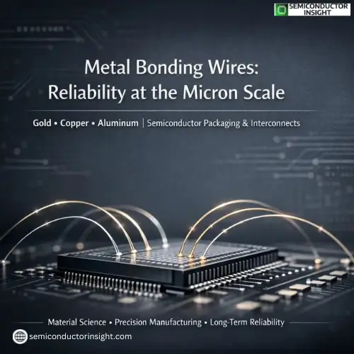
- Metal bonding wires are ultra-thin conductors used to connect semiconductor dies to package leads or substrates. Gold, copper, aluminum, and increasingly alloyed compositions dominate this space, each selected based on conductivity, corrosion resistance, thermal behavior, and cost considerations.
- Unlike commoditized electronic components, bonding wires operate in a quality-driven ecosystem. Even microscopic inconsistencies can compromise yield, making supplier credibility and metallurgical control central to purchasing decisions.
Why Bonding Wire Demand Remains Structurally Strong?
Despite growing interest in flip-chip and wafer-level packaging, wire bonding continues to account for a substantial share of semiconductor interconnects. Its advantages include proven reliability, flexible design compatibility, and lower tooling costs for a wide range of device types.
Power devices, automotive electronics, sensors, memory modules, and industrial control chips still rely heavily on wire bonding. As electric vehicles, renewable energy systems, and industrial automation expand, demand for robust interconnection solutions rises alongside them.
Material Evolution Is Shaping Competitive Positioning
Gold bonding wires once dominated the market due to unmatched stability and process familiarity. However, price volatility and cost pressure have accelerated the shift toward copper and silver-based alternatives. Copper wires offer higher electrical conductivity and better resistance to electro migration, making them suitable for high-current applications.
Manufacturers are now differentiating through surface treatments, alloy optimization, and diameter control rather than raw material choice alone. The market is gradually moving from material substitution toward performance engineering.
Precision Manufacturing as a Market Barrier
Producing bonding wires is not a scale game it is a consistency challenge. Drawing wires to diameters thinner than a human hair while maintaining uniform tensile strength requires specialized equipment and deep process expertise.
This technical barrier limits rapid market entry, reinforcing long-term supplier relationships. Semiconductor fabrications prioritize reliability over experimentation, which stabilizes demand for established producers even during cyclical downturns.
Recent Developments:
- For instance, in August 2025, Tanaka Precious Metal Technologies and Tanaka Electronics made their debut at SEMICON India 2025, which took place in New Delhi. The company showcased a broad portfolio of advanced semiconductor materials which aimed at supporting India’s expanding semiconductor industry with cutting-edge solutions ranging from bonding wires to precious metal recycling.
Regional Manufacturing Dynamics
Asia-Pacific continues to anchor production and consumption, driven by semiconductor assembly concentration in China, Taiwan, South Korea, and Southeast Asia. However, reshoring initiatives and supply chain diversification efforts are encouraging capacity expansion in North America and parts of Europe.
These shifts are influencing procurement strategies, with buyers increasingly valuing geographic redundancy and supply continuity alongside pricing.
How End-Use Applications Are Redefining Specifications
Automotive electronics and power semiconductors are pushing bonding wire requirements beyond traditional benchmarks. Higher operating temperatures, vibration resistance, and extended lifecycle expectations are forcing suppliers to redesign alloys and coatings.
At the same time, consumer electronics prioritize miniaturization and bonding speed, creating parallel demand streams that reward suppliers capable of serving both extremes.
Select Market Forces at Work
Rather than listing conventional drivers, the market is best understood through its operational realities:
- Yield sensitivity ensures consistent demand for premium-grade wires
- Thermal management requirements influence material adoption
- Cost engineering pressures accelerate alloy innovation
These forces operate continuously, shaping supplier strategies without dramatic structural disruption.
Innovation without Visibility, Impact without Headlines
Unlike chip designs that capture attention, bonding wire innovation happens quietly. Improvements are measured in microns, adhesion strength, and failure rate reduction. Yet these incremental advances collectively support the performance gains seen across modern electronics.
Future development is expected to focus on ultra-fine wires for dense packaging, improved oxidation resistance for harsh environments, and compatibility with hybrid packaging architectures.
Feel Free to Reach Our Most Recent Updates of the Report:
https://semiconductorinsight.com/report/global-metal-semiconductor-bonding-wire-market/
Why This Market Continues to Matter?
Metal semiconductor bonding wire market proves that not every critical technology is new or flashy. Some endure because they work reliably, efficiently, and at scale. As long as semiconductors remain central to global technology, bonding wires will continue to play a foundational role in keeping circuits connected and devices functioning.
In order to fulfil the demands of contemporary semiconductor applications, the metal semiconductor bonding wire market has quietly evolved through material innovation and precise manufacturing, continuing to be a key component of electronic packaging.
Comments (0)