
Innovations in Semiconductor Fabrication Changing Novel Ionic Photoacid Generators (PAGs) Market
Modern semiconductor manufacturing relies on highly specialized chemical materials that can respond precisely to light during photolithography. One of the most critical components inside photoresists is the Photoacid Generator (PAG), a compound that releases strong acids when exposed to ultraviolet or extreme-ultraviolet radiation. These acids trigger chemical reactions in the resist layer, allowing nanoscale circuit patterns to form on silicon wafers.
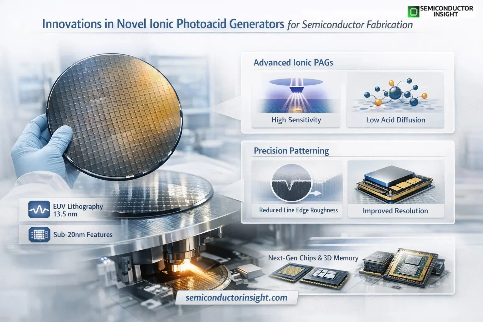
As chip architectures approach sub-10 nanometer nodes, conventional PAG chemistries are being replaced by novel ionic PAG structures that offer higher sensitivity, lower line-edge roughness, and improved lithographic resolution. These molecular systems are designed to control acid diffusion, a key parameter that determines pattern accuracy and feature fidelity during semiconductor fabrication.
Recent studies show that EUV lithography operates at wavelengths of around 13.5 nm, enabling chip patterning with critical dimensions below 20 nm. Such small geometries require photoresist materials with extremely precise photochemical reactions, which has accelerated research into ionic and polymer-bound PAG technologies.
Engineering Ionic PAGs for Precision Lithography
Traditional photoacid generators were primarily based on sulfonium or iodonium salts, which release acid upon photodecomposition. However, newer ionic PAG systems incorporate tailored counter-ions and polymer-bound architectures that significantly improve performance in chemically amplified resists.
In advanced resist formulations, PAG concentrations often range between 8-10 wt% within the photoresist composition to balance sensitivity and pattern resolution. Experimental resist coatings applied to 200 mm silicon wafers can form thin films around 100 nm thickness, enabling precise photolithographic pattern transfer during semiconductor fabrication processes.
Polymer-bound PAG materials have demonstrated notable improvements in photospeed and pattern stability compared with conventional blends. Laboratory experiments have shown that such materials can produce sub-100 nm features with reduced line edge roughness and improved lithographic performance.
These advances are especially important as semiconductor fabs move toward next-generation memory and logic chips requiring extremely small feature sizes and tight process windows.
EUV Lithography Driving Material Innovation
- The shift to EUV lithography is a major technological catalyst for new PAG chemistry. Unlike older deep-ultraviolet processes operating at 248 nm or 193 nm wavelengths, EUV systems require materials capable of absorbing high-energy photons while maintaining minimal stochastic defects.
- Industry testing indicates that new PAG molecules designed for EUV applications can reduce acid diffusion rates significantly, improving resolution-line-edge-sensitivity performance. Such innovations help maintain feature accuracy in dense chip architectures used for AI processors, high-performance computing systems, and advanced memory devices.
- Technological adoption statistics also illustrate the rapid evolution of lithography materials. Around 10% of PAG usage still supports legacy I-Line lithography, while approximately 5% is dedicated to EUV photoresists, reflecting the early but rapidly expanding role of EUV-specific materials in semiconductor manufacturing.
- Meanwhile, experimental lithography systems have demonstrated exposure doses below 12 mJ/cm² and pattern resolutions approaching 25 nm half-pitch, highlighting how advanced resist chemistry and PAG design are pushing the limits of nanoscale fabrication.
Industrial Research and Semiconductor Ecosystem Collaboration
Major semiconductor material developers and chemical manufacturers are investing heavily in next-generation PAG technologies to support advanced nodes below 7 nm. Collaborative development programs between chip foundries, material suppliers, and lithography equipment manufacturers are accelerating innovation.
For instance, some high-purity PAG products designed for advanced semiconductor nodes achieve purity levels above 99.99%, minimizing contamination risks in ultra-clean fabrication environments. In leading semiconductor manufacturing ecosystems, specialized PAG formulations also support resolution improvements that reduce line-edge roughness to ≤0.5 nm, a critical factor for next-generation logic chips.
Another emerging trend is the integration of artificial intelligence in chemical discovery. Machine learning models are now being used to generate and evaluate new PAG molecules by predicting photochemical behavior and acid generation efficiency before laboratory synthesis. This approach can significantly shorten research timelines and accelerate the discovery of optimized molecular structures.
At last, for more in-depth information, don’t forget to read our most recent exclusive report: https://semiconductorinsight.com/report/global-novel-ionic-photoacid-generators-pags-market/
Expanding Applications across Advanced Semiconductor Nodes
Novel ionic PAG materials are enabling semiconductor manufacturing to move toward increasingly complex architectures. These include advanced logic processors, 3D NAND memory structures, and emerging chiplet-based computing platforms.
In modern fabrication environments, photoresist chemistry must simultaneously deliver high resolution, high sensitivity, and excellent etch resistance. Ionic PAG systems are particularly effective because they allow controlled acid generation while minimizing diffusion, helping maintain accurate pattern edges in dense circuit layouts.
Experimental EUV resist systems using these advanced materials have demonstrated significant improvements in lithographic performance metrics, making them promising candidates for future semiconductor manufacturing processes.
As semiconductor technology continues to scale toward angstrom-level nodes, innovations in ionic PAG chemistry will remain central to photolithography advancements. The ongoing convergence of materials science, photochemistry, and semiconductor engineering is therefore shaping the technological trajectory of the Novel Ionic Photoacid Generators (PAGs) Market, positioning it as a crucial component of next-generation chip fabrication.

Comments (0)