
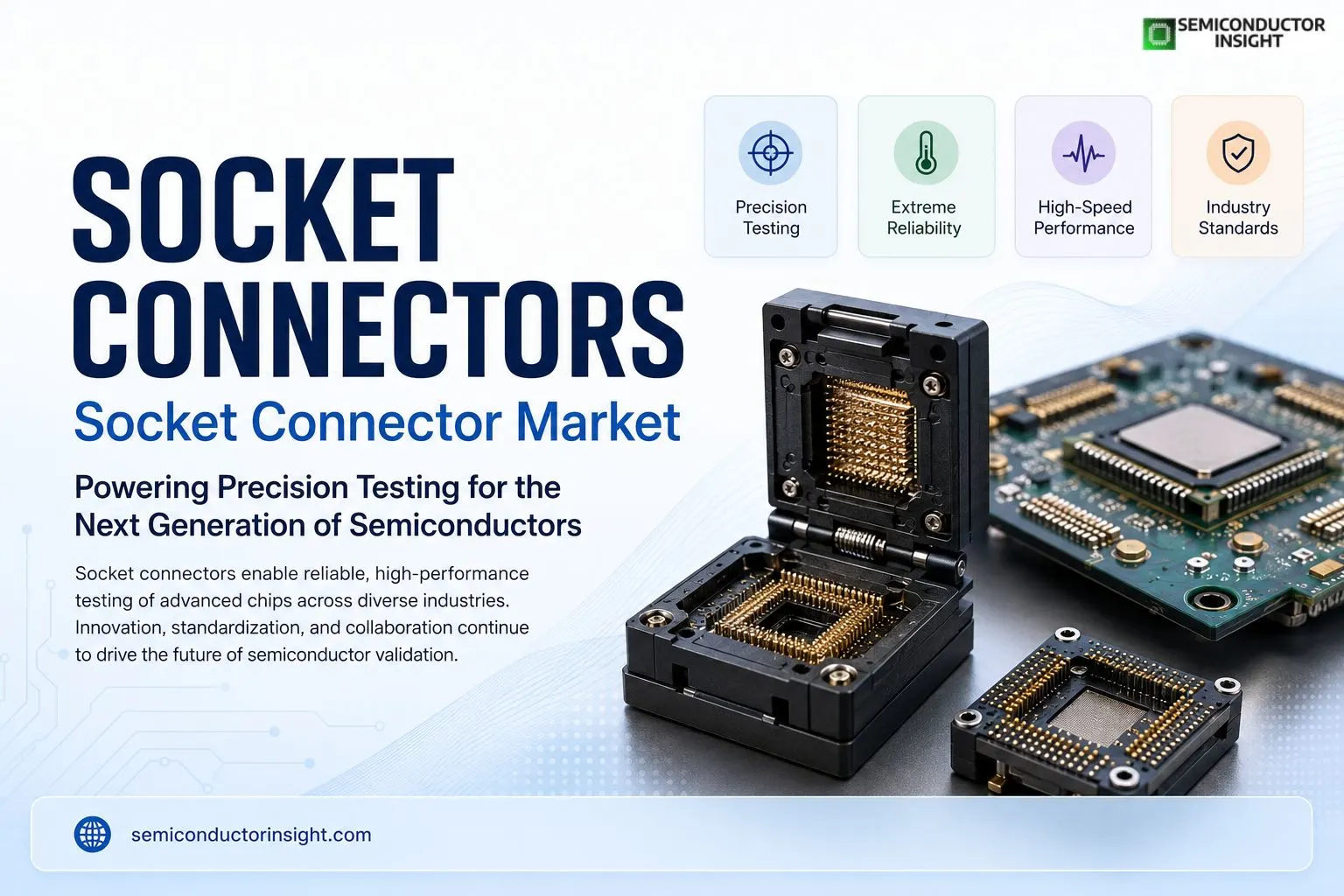
How Socket Connectors Enable Next-Generation Chip Testing in the Socket Connector Market?
Socket connectors serve as critical interfaces in semiconductor manufacturing, allowing temporary electrical connections for testing integrated circuits without permanent soldering. These precision components ensure chips undergo rigorous validation before reaching end users in everything from smartphones to data centre servers.
Precision Contacts Handling Extreme Conditions
Engineers design modern sockets to withstand thousands of insertion cycles while maintaining stable contact resistance often below 50 milliohms. In burn-in applications, manufacturers subject devices to elevated temperatures around 150 degrees Celsius for over 1000 hours under electrical bias.
One case involving PEEK machined housings for automotive IC qualification demonstrated zero socket-related failures across 2000-hour runs, with contact retention force staying within plus or minus 5 per cent across 144 pins.
- High Frequency Performance for Advanced Nodes
- As frequencies climb into millimetre wave ranges, sockets must minimise signal loss and crosstalk.
- Companies like Smiths Interconnect developed coaxial solutions such as the DaVinci Gen V series supporting speeds up to 224 Gbps PAM4 and bandwidth beyond 84 GHz at minus 1 dB insertion loss.
- These sockets incorporate spring probes with gold-plated homogeneous alloys delivering consistent performance for AI accelerators and 6G-related components.
- Fine Pitch and High Density Adaptations
- Semiconductor packages continue shrinking with ball pitches dropping toward 0.15 millimetres.
- Three-dimensional MEMS coaxial sockets fabricated through processes at institutions like Yonsei University address these demands by providing impedance-matched paths for high-density testing.
- Such innovations reduce planarity deviations that could otherwise cause millions in yield losses during validation of high I/O devices exceeding 20000 connections.
- Wafer Level and Chiplet Testing Innovations
- Aehr Test Systems received follow on orders in 2026 for their FOX XP wafer level burn in platforms using proprietary WaferPak contactors.
- These systems enable full wafer electrical contact before singulation helping identify infant mortality failures in silicon photonics and power devices.
- The approach lowers overall manufacturing costs while improving long term reliability for AI and automotive applications.
Material and Thermal Management Advances
Polyether ether ketone or PEEK materials offer excellent thermal stability and chemical resistance making them ideal for socket housings in harsh test environments.
Custom CNC machined components maintain dimensional accuracy across wide temperature swings preventing solder bridge risks in land grid array configurations. iNEMI roadmaps highlight socket heights potentially decreasing to 1.5 millimeters as data rates reach 128 Gbps driving needs for uniform coefficient of thermal expansion materials.
Applications Spanning Industries
Socket connectors have evolved far beyond their traditional role of providing simple electrical connections. In modern data centers, they serve as the backbone for high-performance CPUs, GPUs, and AI accelerators that demand exceptional signal integrity and robust power delivery. With next-generation processors consuming more than 600 watts, advanced socket designs are being paired with improved power interfaces such as the 12V-2×6 connector, which addresses reliability concerns associated with earlier connector generations. These innovations support the growing computational needs of cloud computing, artificial intelligence, and high-performance computing (HPC) environments.
In the aerospace and defense sectors, socket connectors are engineered to withstand harsh operating conditions, including extreme temperatures, vibration, shock, and electromagnetic interference. High pin-count board-to-board connectors designed to meet MIL-STD specifications ensure uninterrupted communication in avionics, radar systems, satellites, and mission-critical defense electronics. Meanwhile, the automotive industry increasingly relies on specialized burn-in and test sockets during semiconductor validation. These sockets help verify the reliability of chips used in electric vehicles (EVs), battery management systems, infotainment platforms, and Advanced Driver Assistance Systems (ADAS), supporting compliance with stringent functional safety standards such as ISO 26262 ASIL-D.
Standardization Efforts Strengthening the Semiconductor Ecosystem
- As semiconductor devices become more complex, standardization is playing an increasingly important role in ensuring compatibility and improving manufacturing efficiency.
- Industry innovators, including companies such as Ampere Computing, have explored advanced elastomer-based socket technologies for large-format processors that require high contact density and exceptional electrical performance.
- These sockets are designed to maintain stable electrical connections throughout demanding validation cycles while minimizing signal loss and mechanical wear.
- Standardized socket platforms are now widely used across multiple stages of semiconductor development, including engineering validation, automatic test equipment (ATE), final production testing, system-level testing (SLT), and High Temperature Operating Life (HTOL) reliability assessments.
- By using consistent socket architectures across these testing environments, manufacturers can reduce development timelines, improve measurement consistency, and simplify data comparison between qualification stages.
- This unified approach not only lowers engineering costs but also accelerates the introduction of new semiconductor products into commercial production while maintaining high quality standards.
To Know More about the Report, You Can Freely Browse Our Latest Updated Report: https://semiconductorinsight.com/report/socket-connector-market/
Ongoing Global Collaboration Driving Next-Generation Socket Innovation
Innovation in socket connector technology continues to advance through close collaboration among semiconductor manufacturers, research institutions, equipment suppliers, and international standards organizations. Universities are conducting research on advanced contact materials, thermal management techniques, and next-generation packaging solutions, while foundries and assembly partners work to optimize socket compatibility with increasingly sophisticated chip architectures.
These collaborative efforts have become especially important as the industry transitions toward chiplet-based architectures, heterogeneous integration, and advanced packaging technologies such as 2.5D and 3D ICs. Socket connectors are also evolving to support high-frequency RF devices, silicon photonics, AI processors, and advanced memory technologies that require greater bandwidth and lower signal latency. Through shared roadmaps, open engineering standards, and cross-industry partnerships, the global semiconductor ecosystem continues to refine socket technologies that enable more reliable testing, faster product development, and improved performance across next-generation electronic devices.

Comments (0)