
How Semiconductor Innovation Is Rebuilding the Biometric Systems Market around Faster Identity Verification?
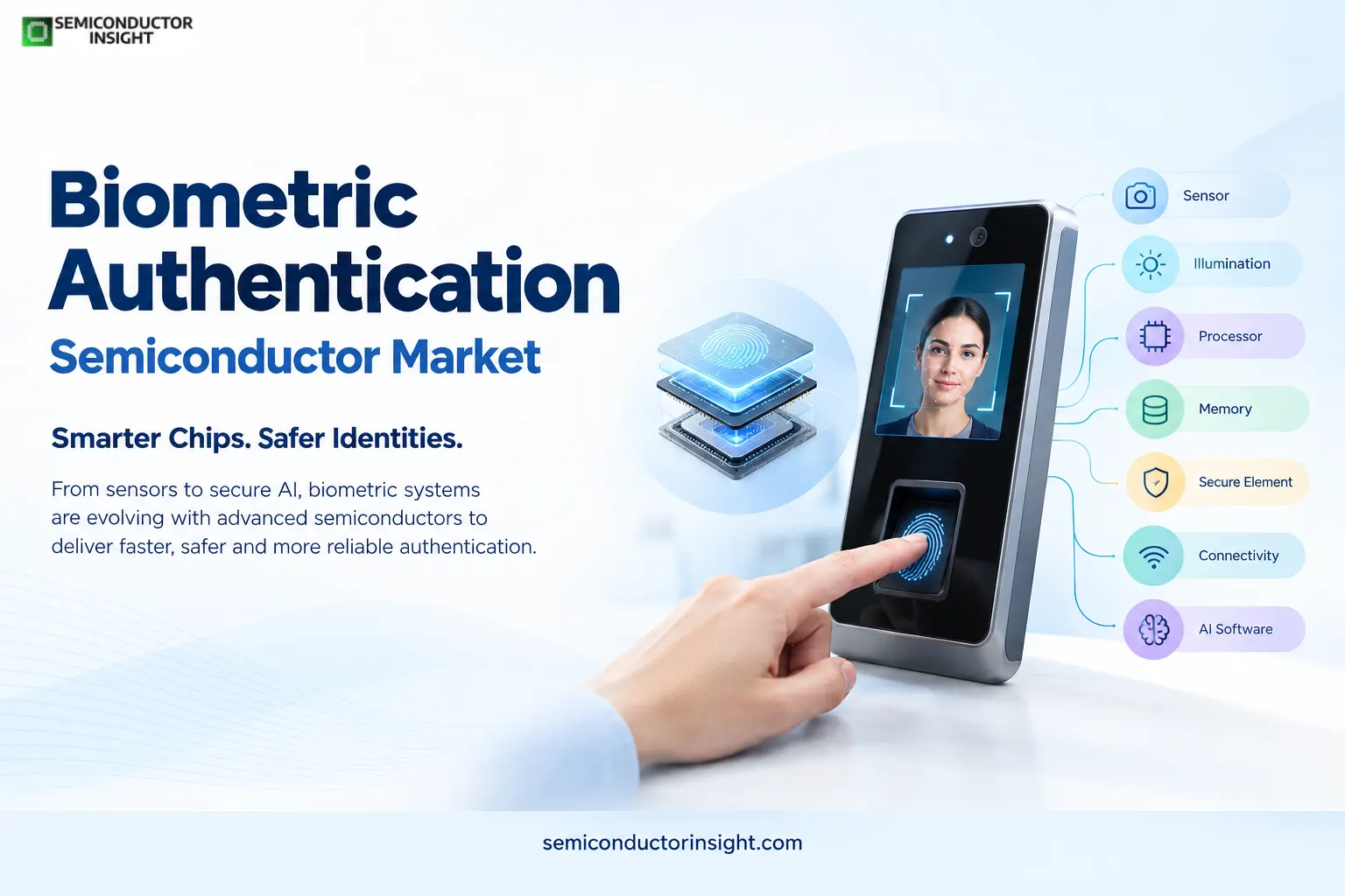
Biometric authentication has moved far beyond the traditional fingerprint scanner. A modern system can involve an image sensor, illumination source, analog front end, processor, memory, secure element, connectivity module and AI software before an authentication decision reaches an application.
That makes biometrics increasingly relevant to semiconductor development. Fingerprint, iris and facial recognition systems depend on the quality of captured data and the processing architecture used to interpret it. NIST specifically notes that biometric performance depends on the quality of the acquired sample and continues to evaluate fingerprint, face and iris technologies through dedicated testing programs.
A New Hardware Architecture Is Taking Shape
The direction of development is shifting toward processing more biometric information directly within trusted hardware. Instead of sending every raw biometric image to a remote environment, systems can perform portions of image enhancement, liveness detection, feature extraction and matching locally.
This architecture can be represented as:
Sensor capture → Image conditioning → Edge AI processing → Liveness check → Secure matching → Authentication decision
The semiconductor components determine how quickly and securely this chain can operate while keeping power consumption within the limits of smartphones, access terminals, and payment devices and embedded systems.
India Demonstrates the Scale of Real-World Deployment
- India provides one of the clearest examples of biometric infrastructure operating at national scale.
- In March 2026, India’s Ministry of Electronics and Information Technology reported approximately 134 crore, or 1.34 billion, live Aadhaar holders and more than 17,000 crore authentication transactions completed by the Aadhaar ecosystem. Authentication can use fingerprint, iris, face, OTP or demographic information depending on the authorized service.
- The scale creates demanding semiconductor requirements. Authentication devices have to operate reliably across different environments while protecting biometric information against replay and tampering.
- UIDAI’s current registered-device architecture distinguishes between L0 and L1 devices. L1 devices perform encryption within a Trusted Execution Environment and use secure hardware elements and enhanced liveness detection.
The Fingerprint Sensor Is Becoming More Intelligent
Fingerprint hardware is moving from passive image acquisition toward active quality assessment and anti-spoofing. NIST’s fingerprint technology work covers optical, solid-state, swipe and other sensor approaches, while its ongoing research also examines contactless fingerprint capture and interoperability with existing systems.
A particularly interesting development came from UIDAI’s 2025 biometric SDK benchmarking initiative. The program tested fingerprint matching for children aged 5–10 using a dataset containing samples separated by a 5–10-year interval, allowing researchers to examine how verification performance changes as fingerprints develop with age.
This illustrates why biometric semiconductor design increasingly requires more than higher sensor resolution. Real-world variability has to be considered at the capture and processing stages.
Facial Recognition Is Driving Computational Requirements
Face authentication places different demands on silicon. Cameras must capture usable images under changing illumination, orientation and distance, while processors need to execute increasingly sophisticated algorithms.
NIST’s evaluation programs measure factors including accuracy, throughput, reliability and sensitivity to image characteristics. The organization also emphasizes that recognition error rates do not reach zero and that performance depends on capture conditions and system thresholds.
For semiconductor developers, this creates demand for image signal processing, neural-processing capabilities, memory bandwidth and hardware security working together inside increasingly compact devices.
Our most recent updated related study is available for free at this link: https://semiconductorinsight.com/report/biometric-systems-market/
2026 Brings a New Standardization Milestone
A significant current development is NIST’s publication of ANSI/NIST-ITL 1-2025 in March 2026. The specification addresses formats for exchanging fingerprint, facial and other biometric information. NIST also reported in June 2026 that work had commenced on an additional 2026 addendum.
Standards such as these matter to semiconductor-enabled biometric systems because interoperability depends on consistent ways of representing and exchanging biometric information.
Multimodal Authentication Is Becoming a System-Level Strategy
A single biometric modality does not work equally well in every situation. Fingerprints can be affected by worn or damaged skin, faces can be affected by lighting or camera position, and iris capture requires appropriate imaging conditions.
Consequently, systems increasingly combine modalities or provide alternatives. UIDAI, for example, has integrated facial biometrics alongside fingerprint and iris modalities for biometric deduplication. It’s reported ABIS architecture is designed to process more than 1 million packets of daily traffic while incorporating liveness and quality checks.
The semiconductor implication is significant: one authentication platform may need to support multiple sensors, processors and security functions rather than one dedicated biometric input.
Security Is Moving Inside the Silicon
- The most important technological shift may be the movement of security closer to the sensor and processor. Secure elements, trusted execution environments, hardware-backed keys and on-device anti-spoofing reduce dependence on software-only protection.
- UIDAI’s L1 registered devices demonstrate this architecture by using secure hardware elements, on-device encryption and liveness mechanisms.
- For biometric semiconductor systems, this creates a convergence between sensing, AI processing and hardware security. The chip is increasingly responsible not only for recognizing a person but also for protecting the process through which recognition takes place.
The Next Generation Will Be Judged at the Point of Capture
The biometric systems market is increasingly becoming a semiconductor story because authentication quality begins before an algorithm produces its final decision. Sensor quality, illumination, processing speed, secure memory, liveness detection and hardware-backed protection all influence the outcome.
With national-scale deployments such as Aadhaar, continuing NIST performance and interoperability work, and newer device architectures built around trusted hardware, biometric technology is moving toward compact systems that can sense, analyze and protect identity information within the same hardware ecosystem.

Comments (0)