
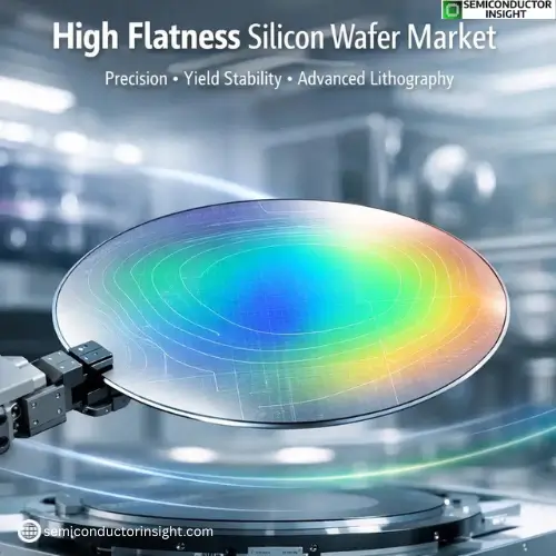
High Flatness Silicon Wafer Market Growth Fueled by Nano electronics Demand
Why Flatness Has Become a Strategic Requirement?
Silicon wafers have always been the backbone of semiconductor manufacturing, but flatness has now become a decisive performance parameter rather than a quality checkpoint. As chipmakers push toward smaller geometries, multi-layer stacking, and tighter overlay tolerances, even microscopic surface deviations can disrupt yield, alignment, and device reliability.
High Flatness Silicon Wafer Market addresses this precision gap by supplying wafers engineered to meet stringent global flatness and site flatness specifications required for advanced lithography, etching, and deposition processes. This market no longer serves only cutting-edge logic fabrications; it increasingly supports memory, power electronics, and specialty semiconductor applications.
What Defines High Flatness in Today’s Fabrication Environment?
High flatness silicon wafers are manufactured to maintain minimal total thickness variation (TTV), global flatness, and site flatness across the entire wafer surface. These parameters ensure consistent photoresist coating, accurate pattern transfer, and stable layer stacking during high-resolution fabrication steps.
As production lines move toward EUV lithography and high-aspect-ratio structures, wafer flatness directly influences throughput efficiency and defect density.
Market Prospects: Accuracy as a Long-Term Growth Foundation
High Flatness Silicon Wafer Market is positioned for steady expansion, anchored by structural changes in semiconductor manufacturing rather than short-term demand cycles. As device geometries shrink and fabrication complexity rises, flatness will remain a non-negotiable requirement.
Growth momentum will be sustained by:
- Continued scaling of advanced logic nodes
- Expansion of power electronics production
- Increasing reliance on multi-layer and heterogeneous integration
Flow of Value Creation in the High Flatness Wafer Ecosystem
Crystal Growth Control → Advanced Wafer Polishing → Metrology & Flatness Mapping → Lithography Accuracy → Yield Stability → Device Performance
This sequence highlights that flatness is not an isolated material property; it is embedded across the entire semiconductor value chain.
Recent Industry Situations Reinforcing Market Demand
Over the past few years, leading semiconductor manufacturers have expanded investment in advanced nodes, power device scaling, and heterogeneous integration. These shifts have placed renewed focus on wafer surface integrity.
In power electronics, especially silicon-based power devices for electric vehicles and renewable energy systems, flatness consistency supports tighter die placement and improved thermal management.
Demand Sources Shaping the Market Landscape
Rather than being driven by a single application, demand for high flatness wafers emerges from multiple technology transitions occurring in parallel.
Key demand contributors include:
- Advanced logic manufacturing using EUV lithography
- High-density memory architectures requiring precise layer alignment
- Automotive and industrial power semiconductors prioritizing reliability
This diversity helps stabilize the market against short-term fluctuations in any one semiconductor segment.
Manufacturing Complexity as a Market Differentiator
Producing high flatness silicon wafers requires tightly controlled crystal pulling, precision grinding, chemical-mechanical polishing, and advanced metrology. Minor variations in temperature gradients or polishing pressure can translate into unacceptable flatness deviation.
As a result, process know-how and equipment integration play a greater role than raw silicon availability. This technical barrier limits new entrants and strengthens the position of established wafer manufacturers with long-term customer qualification histories.
Feel Free to Reach Our Most Recent Updates of the Report:
https://semiconductorinsight.com/report/high-flatness-silicon-wafer-market/
Relationship-Driven Procurement Behavior
Purchasing decisions in this market are rarely transactional. Semiconductor fabs typically qualify wafer suppliers over extended periods, validating flatness consistency across multiple production lots.
Once approved, supplier relationships tend to be long-standing due to:
- Process tuning aligned with fab equipment
- Predictable wafer behavior during critical steps
- Reduced risk of yield loss
This dynamic supports recurring revenue streams rather than spot-market volatility.
Regional Manufacturing Influence
East Asia continues to dominate consumption due to its concentration of advanced fabs, while North America and Europe remain important for specialty semiconductor production and R&D-driven demand. Regional expansion is closely tied to new fab construction, government incentives, and long-term capacity planning.
As more countries invest in domestic semiconductor ecosystems, local availability of high flatness wafers is becoming strategically important, especially for advanced manufacturing independence.
Innovation beyond Surface Smoothness
The next phase of market evolution extends beyond flatness alone. Wafer suppliers are increasingly integrating flatness optimization with:
- Reduced defect density
- Improved edge geometry
- Enhanced mechanical strength
These attributes collectively support thinner wafers and more complex device architectures without compromising handling stability.
Important Lessons for Industry Participants
High flatness silicon wafers are no longer supporting materials; they are enablers of next-generation semiconductor performance. Market success depends on precision engineering, process consistency, and long-term collaboration between wafer suppliers and device manufacturers.

Comments (0)