

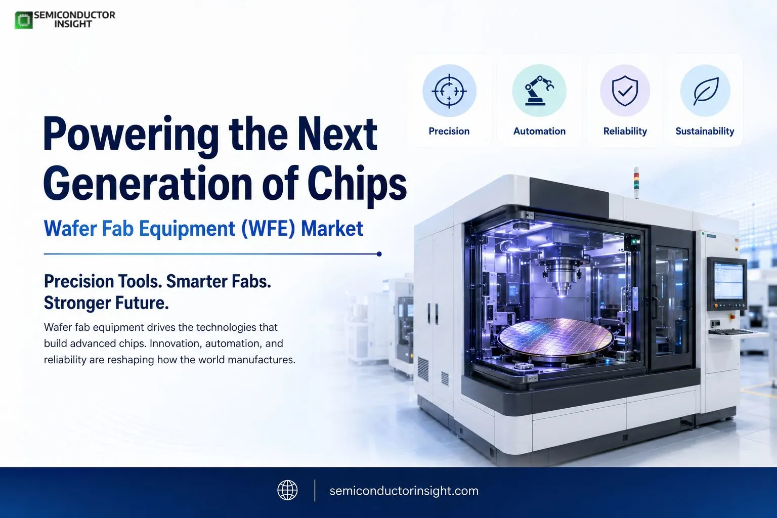
Global Wafer Fab Equipment Surge 2026: Powering Next Generation Chip Production Lines
The wafer fab equipment sector stands at the heart of semiconductor manufacturing, delivering the specialized tools that etch, deposit, and pattern silicon wafers into powerful integrated circuits.
As demand for advanced chips accelerates through artificial intelligence, high performance computing, and next generation communications, these machines represent massive capital investments that shape entire supply chains.
How Are High NA EUV Systems Transforming Wafer Processing Capabilities Today?
· High numerical aperture extreme ultraviolet lithography tools from ASML have moved from research labs into early production environments.
· Intel deployed its first commercial High NA EUV system in late 2025, supporting development for the 14A process node with finer resolution down to around 8 nanometer features.
· TSMC and Samsung are evaluating timelines for broader adoption amid cost considerations, while these machines cost hundreds of millions each and enable patterning at scales previously unattainable with previous generation scanners.
· This technology leap allows chipmakers to continue shrinking transistors while improving performance and power efficiency.
· A single High NA tool can handle complex multilayer exposures with greater precision, reducing the number of process steps in some cases and boosting overall fab productivity for leading edge logic and memory devices.
Emerging Patterns in Advanced Node Equipment Deployment across Key Players
TSMC has been ramping capacity in Arizona alongside its Taiwan operations, incorporating newer lithography and process tools to serve both local and international customers. Intel’s expansions in Ohio, Arizona, and other sites focus on bringing cutting edge logic production onshore, relying heavily on equipment from suppliers like Applied Materials, Lam Research, and ASML. Samsung continues investments in South Korea and the United States for memory and foundry production, pushing boundaries in high bandwidth memory technologies essential for AI servers.
These deployments highlight a shift toward more geographically distributed yet highly specialized manufacturing. New fabs incorporate automation, better contamination control, and energy efficient processes to meet sustainability targets while handling the complexity of sub 5 nanometer and 2 nanometer class technologies.
Why Does Equipment Reliability Matter More Than Ever in Current Production Cycles?
Modern wafer fabs operate in ultra clean environments where even microscopic particles can ruin entire batches worth millions. Equipment suppliers focus on higher uptime, predictive maintenance through sensors and data analytics, and modular designs that allow faster repairs or upgrades without lengthy shutdowns. Tokyo Electron, for instance, has long contributed cluster tools that integrate multiple process chambers efficiently, improving throughput in deposition and etch sequences.
Case studies from ongoing fab builds show that tool availability directly impacts yield learning curves. When new High NA systems arrive, teams spend months calibrating processes, optimizing recipes, and training staff to achieve target production volumes. Delays in any part of the equipment ecosystem can cascade across global chip supplies, as seen in past cycles when lithography tool backlogs affected ramp schedules.
Real World Examples of Fab Equipment Driving Innovation in Specific Applications
ü In memory manufacturing, tools enabling higher aspect ratio etching and advanced deposition support the stacking of more layers in 3D NAND flash, increasing storage density for data centers and consumer devices.
ü For logic chips powering smartphones and automotive systems, precise ion implantation and chemical mechanical polishing equipment ensure uniform doping and planar surfaces critical for transistor performance.
ü Japan’s Rapidus project, backed by government and industry consortiums including Toyota and Sony, installed EUV scanners with plans for high volume production starting around 2027, aiming to strengthen domestic capabilities in advanced semiconductors.
ü In the United States, projects funded through CHIPS incentives include wafer manufacturing and equipment related facilities, contributing to broader ecosystem growth.
You Can Go Through Our Latest Updated Insights Here: https://semiconductorinsight.com/report/wafer-fab-equipment-wfe-market/
Navigating Supply Chain Dynamics and Technology Interdependencies
The concentration of expertise among a handful of equipment leaders creates both strengths and vulnerabilities. ASML maintains a unique position in EUV technology, with systems that require specialized light sources, optics, and infrastructure. Applied Materials and Lam Research dominate in areas like chemical vapor deposition and plasma etch, while KLA excels in metrology and inspection tools needed for process control.
Export controls and geopolitical considerations influence where advanced tools can be shipped, prompting countries to invest in alternative pathways or mature node capabilities. This environment encourages collaboration between governments, equipment makers, and chip manufacturers to secure long term access while fostering innovation in areas like sustainable manufacturing and next generation materials.
Sustainability Shifts Influencing Equipment Design and Operations
Fabs consume enormous amounts of energy, water, and chemicals. Newer equipment generations incorporate features for lower power usage, better waste recovery, and reduced footprint.
Manufacturers work on tools that support more efficient process integration, minimizing the number of steps and resources required per wafer. These improvements become vital as production scales to meet demand for chips in electric vehicles, renewable energy systems, and edge computing devices.
What Lies Ahead for Wafer Fab Equipment Adoption Worldwide
o Ongoing expansions signal sustained investment through the end of the decade and beyond.
o As chip designs grow more sophisticated, equipment must evolve to handle new materials like silicon carbide and gallium nitride alongside traditional silicon.
o The interplay between tool capabilities, process know how, and massive capital commitments will determine who leads in delivering the semiconductors powering tomorrow’s technologies.
This ecosystem remains dynamic, with each new generation of wafer fab equipment unlocking possibilities that ripple through computing, communications, healthcare, and transportation sectors globally.

Comments (0)