

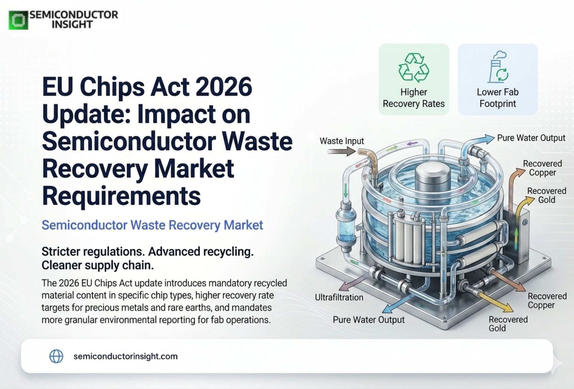
EU Chips Act 2026 Update: Impact on Semiconductor Waste Recovery Market Requirements
Every semiconductor manufacturing facility generates substantial waste streams containing valuable materials that traditional recycling methods often miss. A single PC motherboard holds 566 parts per million gold, 639 ppm silver, and 124 ppm palladium concentrations exceeding typical economic ore grades by more than an order of magnitude.
These precious metals combined represent close to 96% of the non-ferrous focus metal value in printed circuit boards, making semiconductor waste recovery one of the most economically attractive circular economy opportunities in modern manufacturing.
The industry produces over 1 trillion semiconductor devices annually, creating an unprecedented imperative for effective material recovery systems. Semiconductor waste offers concentrated material sources that may be retrieved using sophisticated chemical and mechanical techniques, in contrast to traditional mining operations that necessitate extensive ground removal.
Samsung Cross-Division Circular Resource Model Delivers Galaxy S25 Recycled Components
- Samsung Electronics demonstrated a breakthrough circular economy approach by recycling wafer trays discarded during semiconductor manufacturing into materials used in consumer electronics.
- The company developed recycled plastic from DS Division wafer trays and applied it to Side Keys and Volume Keys of the Galaxy S25 Series, strengthening circular resource processes between divisions.
- The Galaxy S25 features eight different recycled materials across components, including aluminium, rare earth elements like neodymium, and steel, with recycled material integrated into the armour aluminium frame for the first time.
- This cross-divisional strategy earned the Galaxy S25 the 2025 Design for Recycling Award, the highest recognition for leadership in sustainable design.
- The packaging box uses 100% recycled paper, eliminating single-use plastics entirely.
TSMC’s Nearly 90% Water Recycling Rate Establishes Industry Benchmark
Taiwan Semiconductor Manufacturing Company began wastewater recycling in 1995 and developed a proprietary system, achieving nearly 90% recycled wastewater rates, an unmatched level in the industry. TSMC’s major water-consuming process cleans chemical residue on wafer surfaces through ultra-pure water systems, with a three-step strategic approach: controlling pollution by reducing pollutants, recycling pollutants, and recovering pollutants.
The company classifies every wastewater type strictly at process tools, directing flows through distinct piping devices to treatment facilities. Purest water reuses in production scheduling, while poorer grades serve secondary uses like cooling towers and wet scrubbers. An internal 2013 study showed 86.5% process water recycling in 2012, generating 40 million euros in profits and demonstrating economic viability alongside environmental benefits. In 2016, TSMC established Taiwan’s first semiconductor industry recycled water pilot line, and now each drop of water is used an average of 3.5 times.
- Infineon Achieves 80% Carbon Emission Reduction Exceeding 70% Target.
Infineon Technologies reached its 2025 interim goal of reducing carbon emissions by 70% compared to the 2019 base year, achieving an actual reduction of over 80% while doubling revenue. The transition to 100% green electricity translates to an annual avoidance of approximately 975,150 tons of CO₂ equivalents. This accomplishment positions Infineon as a global sustainability leader while demonstrating that emission reductions and business growth can occur simultaneously.
The semiconductor manufacturer’s plans to reduce greenhouse gas emissions by 70% by 2025 set rigorous targets for industry improvement. This performance validates that semiconductor sustainability goals are achievable through systematic operational changes and green energy adoption.
- UL Platinum Zero-Waste-to-Landfill Validation Becomes Industry Standard
Samsung Semiconductor achieved integrated Platinum Zero-Waste-to-Landfill validation for all global sites, the highest grade from the UL certification organisation. The validation evaluates the company’s steps toward the circular economy through waste-to-resource circulation rates, with certification divided into Platinum, Gold, and Silver grades based on the percentage of waste used as resources.
Recovery rates demonstrated include 100% for gold, 95-99% for silver, and 90-94% for certified materials. This certification has become a key indicator for evaluating circular economy progress, with companies increasingly pursuing the Platinum designation as an industry benchmark.
Stay connected for additional in-depth information right here: https://semiconductorinsight.com/report/semiconductor-waste-recovery-market/
Global E-Waste Reaches 62 Million Tonnes, Creating a Recovery Imperative
Worldwide e-waste generation reached a record 62 million tonnes in 2022, up 82% from 2010, and is on track to rise another 32% to 82 million tonnes by 2030. The 62 million tonnes generated in 2022 would fill 1.55 million 40-tonne trucks, forming a bumper-to-bumper line encircling the equator. Worldwide annual e-waste generation rises by 2.6 million tonnes annually, growing five times faster than documented e-waste recycling.
Just 1% of rare earth element demand is met by e-waste recycling, creating a massive opportunity for the semiconductor waste recovery market expansion. In 2022, the world generated 62 million tonnes of e-waste, averaging 7.8 kg per person.
Wafer Reclaim Processes Enable Silicon Reuse in New Manufacturing Cycles
- The Wafer Reclaim and Recovery Market focuses on efficient recycling and reprocessing of silicon wafers as a critical semiconductor industry segment.
- Wafer reclaiming involves cleaning, polishing, and reprocessing used wafers, enabling reuse in manufacturing and testing applications. Recovery extends to extracting valuable materials from discarded wafers, ensuring resource optimisation.
- Researchers demonstrated that sustainable, environmentally friendly recycling methods extract silicon of sufficient purity to reuse in new semiconductor devices.
- This capability closes the manufacturing loop, reducing virgin silicon demand and associated environmental impacts.
European Chips Act Sustainability Enforcement Creates Infrastructure Urgency
Regulations around the globe, such as the European Chips Act, begin focusing on enforcing semiconductor sustainability and encouraging recycling, forcing the industry to create necessary infrastructure quickly. Current processes are often energy-intensive, polluting, and linked to exploitative labour practices, requiring new sustainable technologies and practices for extracting and recycling semiconductors.
The industry must create infrastructure to collect used semiconductors and bring them to recycling locations, with manufacturers introducing circularity through buy-back or collection schemes that recover materials from old semiconductors for new ones.

Comments (0)