
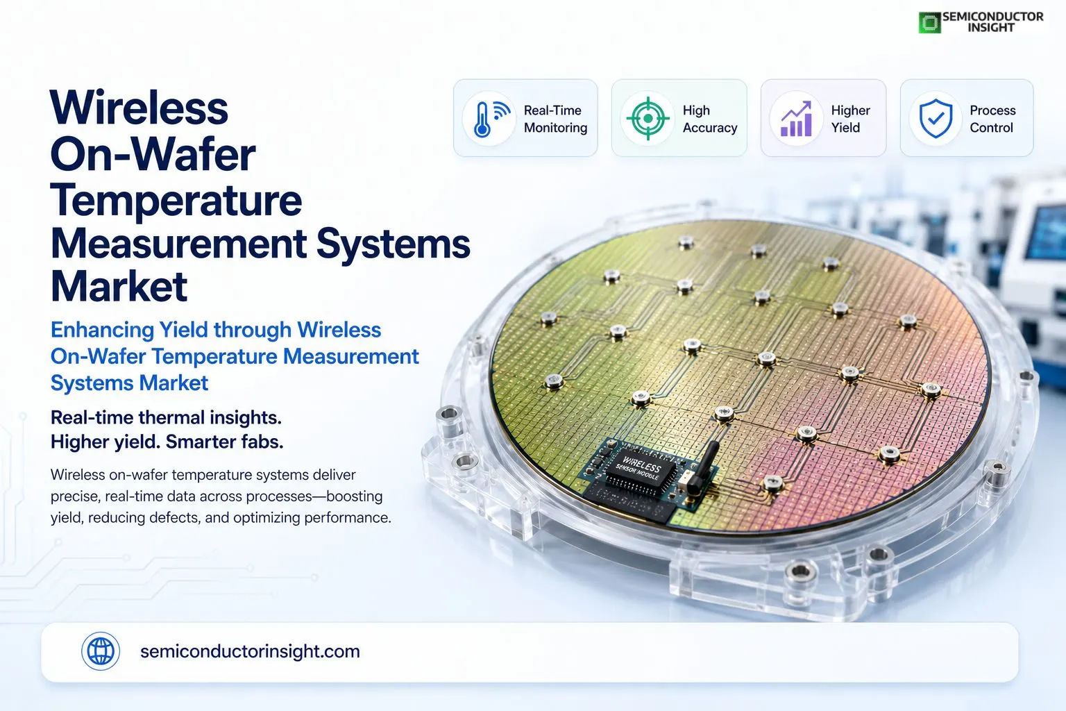
Enhancing Yield through Wireless On-Wafer Temperature Measurement Systems Market Integration Strategies
In the fast-evolving world of semiconductor manufacturing, where even minor temperature fluctuations can scrap entire batches worth millions, engineers are turning to advanced wireless solutions embedded directly into wafer-like carriers.
These systems capture real-time thermal data across production processes without the clutter of wires or the risks of contamination.
How Wireless Integration Is Reshaping Thermal Monitoring in Advanced Nodes?
- Traditional temperature checks often relied on fixed probes or post-process analysis, leaving gaps in understanding what actually happens to a 300mm silicon wafer inside a vacuum chamber or etcher. Wireless on-wafer systems change that by placing multiple high-accuracy sensors sometimes up to 65 points across a dummy or test wafer that mimics production ones.
- Companies like KLA have developed tools such as their ScannerTemp wireless wafer, which delivers detailed spatial and temporal maps during lithography steps. This helps control pattern overlay issues critical for sub-5nm features.
- In one documented approach from research published in MDPI journals, a wireless on-wafer temperature monitoring system (OTMS) used infrared communication and thin lithium batteries to operate safely inside vacuum environments while staying under 1.5mm thick for compatibility with automated wafer handlers.
- Such designs ensure the sensor wafer travels seamlessly through process tools without triggering interlocks or introducing particles.
Live Factory Initiatives Strengthening Defect Reduction in Advanced Chip Plants
Fabs in Asia and North America have integrated these systems for electrostatic chuck (ESC) condition monitoring after repairs. One case involved deploying a system with multiple temperature measurement units to verify uniform heating across repaired chucks, preventing defects in plasma etching.
- In ion implantation and annealing, wireless HighTemp wafers collect data under actual conditions, revealing thermal non-uniformities that affect dopant activation.
- A Berkeley-led study from earlier autonomous sensor work demonstrated wireless reporting at temperatures up to 120°C with real-time transmission, paving the way for modern battery-powered variants that endure full process flows.
Taiwan Semiconductor Manufacturing Company and similar leaders emphasize in-situ monitoring for EUV lithography scanners, where thermal variations as small as fractions of a degree impact overlay accuracy by nanometers. Wireless solutions provide the granular data needed to qualify tools faster and match them across production lines.
Emerging Materials and Sensor Architectures Pushing Performance Boundaries
Recent innovations incorporate RTD (resistance temperature detector) arrays bonded to silicon surfaces for superior accuracy compared to thermocouples. Suppliers offer variants rated from -40°C to over 250°C, with precision reaching 0.05°C in controlled setups. These thin profiles, often below 5mm, include nine or more miniature sensors per wafer for comprehensive mapping.
Integration with automation bases allows data download after each run without manual intervention, supporting lights-out manufacturing goals. Low-temperature versions target cryogenic or specialized etching, while high-temp ones handle rapid thermal processing.
Want to learn more about the report? Check out our latest updated version for free: https://semiconductorinsight.com/report/wireless-on-wafer-temperature-measurement-systems-market/
Smart Fab Expansion and Energy-Efficient Thermal Control in Advanced Semiconductor Manufacturing
- As semiconductor manufacturing facilities expand across the United States, Europe, India, and East Asia under government-backed initiatives such as the CHIPS Act and regional semiconductor incentive programs, wireless on-wafer temperature measurement systems are becoming increasingly important for advanced process qualification and contamination-free metrology.
- Modern fabs producing advanced logic, memory, and AI-focused chips require extremely precise thermal monitoring to maintain yield consistency within highly controlled cleanroom environments.
- At the same time, manufacturers are placing stronger emphasis on operational efficiency and sustainability.
- Real-time wireless thermal measurement helps engineers identify temperature variations and hot spots during etching, deposition, and cleaning processes, allowing process parameters to be adjusted more accurately.
- This improves tool matching across multiple production systems, reduces wafer scrap rates, lowers unnecessary chemical usage, and minimizes energy-intensive over-processing steps.
- Research collaborations in Europe and other semiconductor innovation hubs are also focusing on calibration accuracy and traceability standards for wafer-level wireless sensors, strengthening confidence for deployment in high-mix and next-generation fabrication environments.
- The ability to maintain stable thermal profiles across multiple process chambers is becoming especially valuable as fabs scale production for advanced nodes, high-bandwidth memory, and AI semiconductor manufacturing where even small temperature deviations can directly affect device performance and yield stability.
Integration with AI-Driven Process Analytics
Modern systems feed data into machine learning platforms that predict drifts before they cause defects. Combined with other in-situ sensors, they create digital twins of process chambers. This proactive approach supports the industry’s push toward higher yields at smaller nodes, where thermal budgets are tighter than ever.
Overcoming Integration Hurdles in Diverse Process Flows
- Engineers customize sensor layouts for specific applications dense arrays for uniformity checks in deposition, or targeted placements for edge-effect studies in bevel processes.
- Battery life and data transmission through chamber walls remain focus areas, with infrared and other wireless methods evolving rapidly.
- As 2nm and Angstrom-scale technologies advance, wireless on-wafer temperature measurement systems will play an even bigger role in enabling reliable, high-throughput manufacturing.
- Their ability to deliver production-like insights without disrupting workflows positions them as essential tools for the next decade of semiconductor progress.
These innovations underscore a broader shift toward smarter, more autonomous fabs where data-driven decisions replace guesswork in thermal management. The result is not just better chips, but a more resilient and efficient global supply chain.

Comments (0)