Plasma-Etching Endpoint Detectors Market Insights
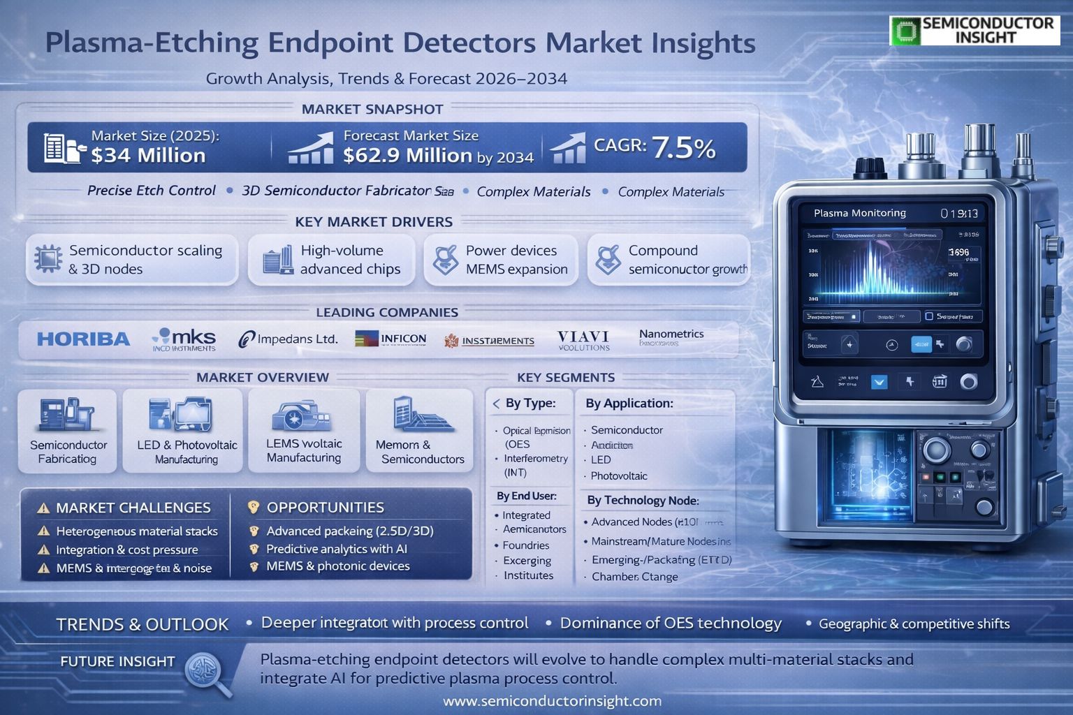
Global Plasma-Etching Endpoint Detectors market size was valued at USD 34 million in 2025. The market is projected to grow from USD 36.6 million in 2026 to USD 62.9 million by 2034, exhibiting a CAGR of 7.5% during the forecast period.
Plasma-etching endpoint detectors are critical metrology tools used in semiconductor fabrication and related industries to precisely determine when an etching process has completed its task on a specific layer of a wafer. These systems monitor real-time changes in the plasma’s optical emission, interferometric signals, or other physical properties to signal the transition from etching the target material to reaching the underlying layer, which is essential for ensuring process control, consistency, and maximizing device yields.
The market is experiencing steady growth driven by several factors, including the relentless advancement of semiconductor nodes requiring atomic-level precision and the expansion of advanced packaging technologies. Furthermore, rising demand for power devices, MEMS sensors, and compound semiconductors for applications like LEDs and photovoltaics necessitates more controlled etching processes. Key players are actively innovating; for instance, companies like HORIBA and MKS Instruments continuously enhance their Optical Emission Spectroscopy (OES) and interferometry solutions to meet the challenges of etching new materials in complex 3D structures. The competitive landscape also includes specialized firms like Impedans Ltd. and Inficon, which contribute to a diverse technological portfolio addressing various application needs across the semiconductor ecosystem.
MARKET DRIVERS
Advancements in Semiconductor Device Scaling and Complexity
The relentless drive toward smaller transistor nodes and 3D device architectures like FinFETs and GAA structures necessitates unprecedented etching precision. This directly fuels demand for advanced plasma-etching endpoint detectors, as they are critical for achieving the necessary etch depth and profile control. Without real-time endpoint detection, yield in advanced logic and memory fabrication would suffer significantly.
Expansion of High-Volume Manufacturing for Advanced Chips
The global ramp in manufacturing capacity for leading-edge semiconductors, including high-performance computing (HPC) chips and advanced DRAM, requires consistent, high-throughput processes. Plasma-etching endpoint detectors enable automated process control and repeatability across thousands of wafers, minimizing human error and maximizing tool utilization in mega-fabs.
➤ A key driver is the integration of endpoint detection data with fab-wide advanced process control (APC) systems, creating a feedback loop for continuous process optimization.
Furthermore, the growth of compound semiconductor manufacturing for 5G RF and power electronics applications presents specialized etching challenges that are increasingly addressed by sophisticated detector technologies, further expanding the served available market.
MARKET CHALLENGES
Technical Complexity in Heterogeneous Material Stacks
As chip designs incorporate diverse new materials,from novel metals to complex low-k dielectrics and etch-stop layers,identifying a clear and unambiguous optical or plasma emission signal for endpoint becomes more difficult. This technical challenge requires continuous R&D into more sensitive sensors and advanced algorithms to parse complex signal data, increasing development costs and time-to-solution.
Other Challenges
Integration and Cost Pressure
Integrating next-generation endpoint detectors into existing etch tools without affecting process stability or requiring costly chamber modifications is a significant hurdle. Additionally, semiconductor manufacturers exert constant cost pressure, demanding higher performance without proportional increases in subsystem cost.
Signal Interference in High-Density Plasmas
Modern high-density plasma sources can generate a high level of broadband emission noise, which can mask the subtle spectral lines that endpoint detectors rely on. This necessitates sophisticated filtering and signal processing technologies to maintain detection reliability.
MARKET RESTRAINTS
Capital Expenditure Cycles and Economic Volatility
The plasma-etching endpoint detectors market is intrinsically linked to the capital investment cycles of semiconductor manufacturers. During periods of economic downturn or reduced chip demand, fab tool purchases and upgrades are deferred or canceled, directly restraining demand for new endpoint detection systems. The high cost of new etch tools, of which detectors are a critical subsystem, makes them susceptible to budget cuts.
MARKET OPPORTUNITIES
Adoption in Advanced Packaging and Heterogeneous Integration
The shift toward advanced packaging schemes like 2.5D/3D ICs and chiplets requires precise etching for through-silicon vias (TSVs) and redistribution layers. This creates a significant new growth avenue for the plasma-etching endpoint detectors market outside traditional front-end wafer fabrication. Detectors ensure the critical etch stopping on barrier layers within these complex packages.
Development of AI-Powered Predictive Analytics
The integration of artificial intelligence and machine learning with endpoint detection systems presents a major opportunity. AI algorithms can analyze historical endpoint data and real-time plasma signals to predict process drift, recommend corrections, and even forecast maintenance needs, moving from reactive detection to predictive process control and offering substantial value to manufacturers.
Growth in the MEMS and Photonics Fabrication Sectors
Beyond mainstream silicon, the fabrication of Micro-Electro-Mechanical Systems (MEMS) and silicon photonics devices relies on highly selective etching processes. The expansion of these application areas, driven by sensors and data communications, provides a dedicated and growing niche for specialized plasma-etching endpoint detector solutions.
Plasma-Etching Endpoint Detectors Market Trends
Technological Integration and Process Control
Endpoint detection (EPD) is a critical component for ensuring consistency and high yields in advanced plasma-etching processes. The primary trend driving the Plasma-Etching Endpoint Detectors Market is the deepening integration of these detection systems with real-time process control frameworks. As semiconductor device structures become more complex and layer thicknesses shrink, the demand for precise and reliable endpoint signals increases significantly. This integration is essential not only for etching through specific wafer layers but also for completing chamber cleaning cycles to prevent cross-contamination between plasma recipes. The market is responding with detectors that offer higher sensitivity and faster response times to meet these stringent manufacturing requirements.
Other Trends
Dominance of Optical Emission Spectroscopy (OES)
The Plasma-Etching Endpoint Detectors Market continues to be shaped by the dominance of Optical Emission Spectroscopy (OES) as the preferred technology. OES systems are favored for their non-invasive nature and ability to monitor multiple chemical species simultaneously during the etch process. This capability is vital for detecting subtle changes in plasma composition that signal an endpoint, particularly in multi-layer and high-aspect-ratio applications. While other methods like interferometry (INT) are used for specific, often transparent, materials, the versatility and proven reliability of OES solidify its leading position across key applications in semiconductor, LED, and photovoltaic manufacturing.
Geographic and Competitive Landscape Shifts
The geographic distribution of the Plasma-Etching Endpoint Detectors Market is evolving, with significant manufacturing and demand concentration in key regions like the United States, China, Japan, and South Korea. This concentration aligns with global semiconductor fabrication capacity. The competitive landscape is structured, with a few key players holding a substantial combined market share. Leaders including HORIBA, MKS Instruments, and Inficon drive innovation, focusing on enhancing detector accuracy and data analytics integration. The trend is toward offering comprehensive solutions that combine endpoint detection with advanced software for yield management and predictive maintenance, moving beyond standalone hardware sales.
COMPETITIVE LANDSCAPE
Key Industry Players
A Consolidated Market Driven by Precision and Process Control
The global plasma-etching endpoint detectors market is characterized by a high degree of technological specialization and is dominated by a handful of established instrumentation leaders. The competitive arena is highly consolidated, with the top five players accounting for a significant share of the global revenue as of recent estimates. HORIBA and MKS Instruments are widely recognized as frontrunners, leveraging their deep expertise in spectroscopic and process control solutions for the semiconductor capital equipment sector. Their dominance is anchored in providing highly reliable Optical Emission Spectroscopy (OES) systems, which represent the most prevalent endpoint detection method. These companies compete primarily on the basis of measurement precision, integration capabilities with leading etch tool platforms, advanced software algorithms for signal analysis, and the robustness of their global technical support networks, which are critical for maintaining high-volume manufacturing yields.
Beyond the market leaders, several significant players operate in specialized or regional niches, contributing to a diverse competitive ecosystem. Companies like Impedans Ltd., with its focus on plasma diagnostics, and Inficon, known for its vacuum and process instrumentation, offer targeted endpoint detection solutions. The market also sees participation from other notable instrumentation and equipment suppliers who provide complementary or alternative detection technologies, such as interferometry-based systems. Competition intensifies as the industry demands detectors capable of handling increasingly complex multi-patterning stacks and novel materials at advanced nodes, pushing all vendors towards continuous R&D investment for enhanced sensitivity and faster response times to secure design wins with leading foundries and memory manufacturers.
List of Key Plasma-Etching Endpoint Detectors Companies Profiled
- HORIBA
- MKS Instruments
- Impedans Ltd.
- Inficon
- Advanced Energy Industries, Inc.
- VIAVI Solutions Inc.
- Nanometrics (now part of Onto Innovation)
- KLA Corporation
- Plasmetrex GmbH
- Corona Optical Systems
- Gamma Instrument Co., Ltd.
- Lasertec Corporation
- Hamamatsu Photonics K.K.
- Oxford Instruments Plasma Technology
- SENTECH Instruments GmbH
Segment Analysis:
| Segment Category | Sub-Segments | Key Insights |
| By Type |
|
Optical Emission Spectroscopy (OES) is the dominant technology due to its real-time, in-situ monitoring capability and high reliability in complex plasma environments.
|
| By Application |
|
Semiconductor manufacturing represents the core application, driving the highest demand and technological innovation for endpoint detectors.
|
| By End User |
|
Foundries are the leading end-user segment, characterized by high-volume, contract-based semiconductor manufacturing.
|
| By Technology Node |
|
Advanced Nodes (<10nm) demand the most sophisticated endpoint detection solutions and represent the key growth frontier.
|
| By Process Stage |
|
Front-End-of-Line (FEOL) Etching is the most critical and demanding stage for endpoint detection technology.
|
Regional Analysis: Global Plasma-Etching Endpoint Detectors Market
Asia-Pacific
The region’s dominance is anchored by the world’s highest concentration of leading-edge semiconductor fabrication plants. These facilities require plasma-etching endpoint detectors for every etch process, driving consistent, high-volume procurement. The ecosystem fosters intense collaboration between detector manufacturers and foundries to develop custom solutions.
National strategies like South Korea’s “K-Semiconductor Belt,” Japan’s semiconductor revival subsidies, and China’s substantial investments under its “Made in China 2025” policy directly stimulate demand. These initiatives fund new fab construction and equipment upgrades, creating a robust market for advanced plasma-etching endpoint detectors.
Asia-Pacific is typically the first region to adopt the newest plasma-etching endpoint detector technologies for high-volume manufacturing. The fast-paced innovation cycle in foundries necessitates detectors with superior sensitivity for complex 3D structures and new materials like high-k dielectrics and metal gates.
A mature local ecosystem of component suppliers and subsystem integrators supports plasma-etching endpoint detector manufacturers. This integration reduces lead times, fosters rapid prototyping for next-generation tools, and enhances technical support for the dense installed base of etch tools across the region’s fabs.
North America
North America remains a critical region in the Plasma-Etching Endpoint Detectors Market, characterized by its role as a global center for R&D, design innovation, and headquarters for major semiconductor capital equipment companies. Demand is driven by leading-edge research at national laboratories, university nanofabrication facilities, and the advanced development fabs of integrated device manufacturers (IDMs). The market here prioritizes plasma-etching endpoint detectors for pioneering new processes, such as those for compound semiconductors, advanced packaging, and power devices. The close collaboration between detector suppliers and tool OEMs in Silicon Valley and other tech hubs accelerates the integration of sophisticated optical emission spectroscopy (OES) and other multi-wavelength detection capabilities into next-generation etch platforms destined for global fabs.
Europe
Europe’s position in the Plasma-Etching Endpoint Detectors Market is defined by technological specialization and high-value manufacturing. The region hosts several world-leading semiconductor equipment manufacturers whose advanced etch tools incorporate proprietary endpoint detection systems. Demand is sustained by niches like automotive semiconductors, MEMS sensors, and power electronics, where precise etch control is paramount. European research institutions and industrial clusters are at the forefront of developing detectors for novel applications, including etching of 2D materials and complex photonic structures. The market is further supported by EU initiatives aimed at bolstering strategic autonomy in microelectronics, which encourage investment in pilot lines and equipment development that rely on precise process monitoring like that provided by plasma-etching endpoint detectors.
South America
The South American market for Plasma-Etching Endpoint Detectors is nascent but emerging, primarily focused on servicing established industrial and academic research facilities rather than high-volume commercial manufacturing. Key demand originates from university cleanrooms and national science institutes in Brazil and Argentina, which utilize plasma-etching endpoint detectors for prototyping and small-scale production of specialized devices. The market dynamics are influenced by regional efforts to build technological capacity in microelectronics, though it remains reliant on imports of full etch tools with integrated detectors. Growth is gradual, tied to broader regional economic factors and incremental investments in upgrading research infrastructure for semiconductor-related studies.
Middle East & Africa
The market for Plasma-Etching Endpoint Detectors in the Middle East & Africa region is currently in a developmental phase, with activity centered on strategic national investments aimed at diversifying economies. Countries like Saudi Arabia and the UAE are making foundational investments in technology hubs and research centers that include semiconductor-focused capabilities. Initial demand for plasma-etching endpoint detectors is thus generated by academic and R&D installations as part of long-term capacity-building goals. While not yet a significant volume market, these strategic initiatives indicate potential future growth corridors as regional partnerships with global technology firms evolve and basic infrastructure for advanced manufacturing is established.
Report Scope
This market research report provides a comprehensive analysis of the Plasma-Etching Endpoint Detectors Market, covering the forecast period 2026–2034. It offers detailed insights into market dynamics, technological advancements, competitive landscape, and key trends shaping the industry.
Key focus areas of the report include:
- Market Overview: The report begins with an overview outlining its current market scenario, key growth indicators, and industry transformation drivers. It discusses macroeconomic factors, demand–supply balance, regulatory landscape, and the strategic role of semiconductors in powering advancements across industries such as automotive, telecommunications, consumer electronics, and industrial automation.
- Market Size & Forecast: Historical data and future projections for revenue, unit shipments, and market value across major regions and segments.
- Segmentation Analysis: Detailed breakdown by product type, technology, application, and end-user industry to identify high-growth segments and investment opportunities.
- Regional Insights: Insights into market performance across North America, Europe, Asia-Pacific, Latin America, and the Middle East & Africa, including country-level analysis where relevant.
- Competitive Landscape: Profiles of leading market participants, including their product offerings, R&D focus, manufacturing capacity, pricing strategies, and recent developments such as mergers, acquisitions, and partnerships.
- Technology Trends & Innovation: Assessment of emerging technologies, integration of AI/IoT, semiconductor design trends, fabrication techniques, and evolving industry standards.
- Market Drivers & Restraints: Evaluation of factors driving market growth along with challenges, supply chain constraints, regulatory issues, and market-entry barriers.
- Stakeholder Insights: Insights for component suppliers, OEMs, system integrators, investors, and policymakers regarding the evolving ecosystem and strategic opportunities.
Primary and secondary research methods are employed, including interviews with industry experts, data from verified sources, and real-time market intelligence to ensure the accuracy and reliability of the insights presented.
FREQUENTLY ASKED QUESTIONS:
What is the current market size of Plasma-Etching Endpoint Detectors Market?
-> Global Plasma-Etching Endpoint Detectors Market was valued at USD 34 million in 2025 and is projected to reach USD 62.9 million by 2034, growing at a CAGR of 7.5% during the forecast period.
Which key companies operate in Plasma-Etching Endpoint Detectors Market?
-> Key players include HORIBA, MKS Instruments, Impedans Ltd., and Inficon, among others. In 2025, the global top five players held a significant revenue share.
What are the key applications of Plasma-Etching Endpoint Detectors?
-> Key applications include Semiconductor, LED, Photovoltaic, and other wafer fabrication processes. Endpoint detection is essential for ensuring process control, consistency, and optimizing device yields.
What are the main types of Plasma-Etching Endpoint Detectors?
-> The market is segmented by type, primarily Optical Emission Spectroscopy (OES), Interferometry (INT), and Others. The OES segment is a key technology in the market.
Which regions are analyzed in this report?
-> The report provides a detailed regional analysis covering North America, Europe, Asia, South America, and the Middle East & Africa, including major countries like the U.S., China, Japan, and Germany.

Get Sample Report PDF for Exclusive Insights
Report Sample Includes
- Table of Contents
- List of Tables & Figures
- Charts, Research Methodology, and more...
 Download Sample Report PDF