
Ceramic Packages Market Analysis Material Science and Semiconductor Integration
Ceramic packages market is gaining strong momentum as semiconductor manufacturers increasingly prioritize thermal stability, electrical reliability, and long-term device performance. Ceramic packaging serves as a protective enclosure for semiconductor chips while enabling efficient electrical connectivity and heat management. These packages create a hermetically sealed environment that protects sensitive electronic components from moisture, chemical contamination, and environmental stress, ensuring device longevity and performance consistency.
Ceramic materials offer greater mechanical strength and stability than conventional plastic packaging, which makes them crucial for high-power electronics, automotive systems, aeronautical devices, and cutting-edge communication technology. The shift toward compact, high-performance electronics continues to drive adoption of ceramic packages across semiconductor manufacturing ecosystems.
Material Science behind Semiconductor Ceramic Packages
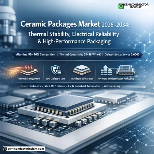
- The foundation of the ceramic packages market lies in advanced electroceramic materials such as alumina, aluminum nitride, and multilayer ceramics. Among these, alumina represents one of the most widely used materials, typically comprising nearly 90% to 96% aluminum oxide composition in semiconductor packages.
- These materials exhibit exceptional electrical insulation, corrosion resistance, and high mechanical strength. Ceramic materials are inorganic, non-metallic substances produced through high-temperature sintering processes that deliver precise dimensional stability and durability.
- Their chemical inertness makes them resistant to oxidation, acids, and environmental degradation, ensuring reliable performance even in extreme industrial conditions. Additionally, aluminum nitride ceramics provide significantly higher thermal conductivity compared to conventional materials, enabling efficient heat removal from semiconductor devices.
- Such advanced material characteristics position ceramic packages as critical enablers of next-generation semiconductor technologies.
Thermal Management Capabilities Driving Market Adoption
One of the most important drivers of the ceramic packages market is efficient heat dissipation. Semiconductor devices generate substantial heat during operation, particularly in power electronics and high-frequency systems. Ceramic materials exhibit superior thermal conductivity, allowing heat to transfer quickly away from chips and preventing performance degradation or failure.
Studies show that high-purity ceramic substrates demonstrate thermal conductivity ranges between 24 to 28 W per meter-Kelvin, significantly improving device lifespan by reducing overheating risks.
This thermal performance supports applications in electric vehicles, renewable energy systems, and industrial automation, where maintaining stable operating temperatures is essential for reliability.
Electrical Insulation and Signal Performance Enhancement
Ceramic semiconductor packages offer high dielectric strength and low signal loss, making them highly suitable for high-frequency and high-voltage applications. Their insulating properties prevent electrical leakage and electromagnetic interference, enabling stable signal transmission in advanced communication systems.
The dielectric loss of certain ceramic materials can be as low as 0.0002 to 0.002 at high frequencies, which significantly improves signal fidelity and operational accuracy in modern semiconductor devices.
Such electrical performance advantages are particularly valuable in 5G communication equipment, RF components, and high-speed computing technologies.
Miniaturization and Structural Reliability in Chip Packaging
Modern semiconductor devices demand increasingly compact and efficient packaging solutions. Ceramic packages support miniaturization through multilayer structures, allowing three-dimensional electrical routing and precise circuit integration.
Their high rigidity prevents warping under thermal stress, while low gas permeability ensures long-term structural stability. These properties make ceramic packaging ideal for applications requiring high reliability, including space electronics and defense systems.
Additionally, ceramic packages maintain dimensional stability across wide temperature ranges, reducing mechanical deformation and improving device lifespan in demanding environments.
For a more thorough report, please contact us using our most recent report:
https://semiconductorinsight.com/report/ceramic-packages-market/
Industrial Applications Expanding Market Potential
The ceramic packages market is closely linked with the expansion of semiconductor applications across multiple industries. These packages are widely used in RF modules, microwave devices, power switching systems, sensors, and optical electronics due to their resistance to extreme temperatures and harsh environmental conditions.
In automotive electronics and industrial machinery, ceramic packaging enhances device reliability by reducing failure rates under continuous mechanical and thermal stress.
Furthermore, emerging technologies such as artificial intelligence computing and advanced sensor systems rely on high-density ceramic packages to optimize thermal efficiency and electrical performance, reinforcing market growth.

Comments (0)