

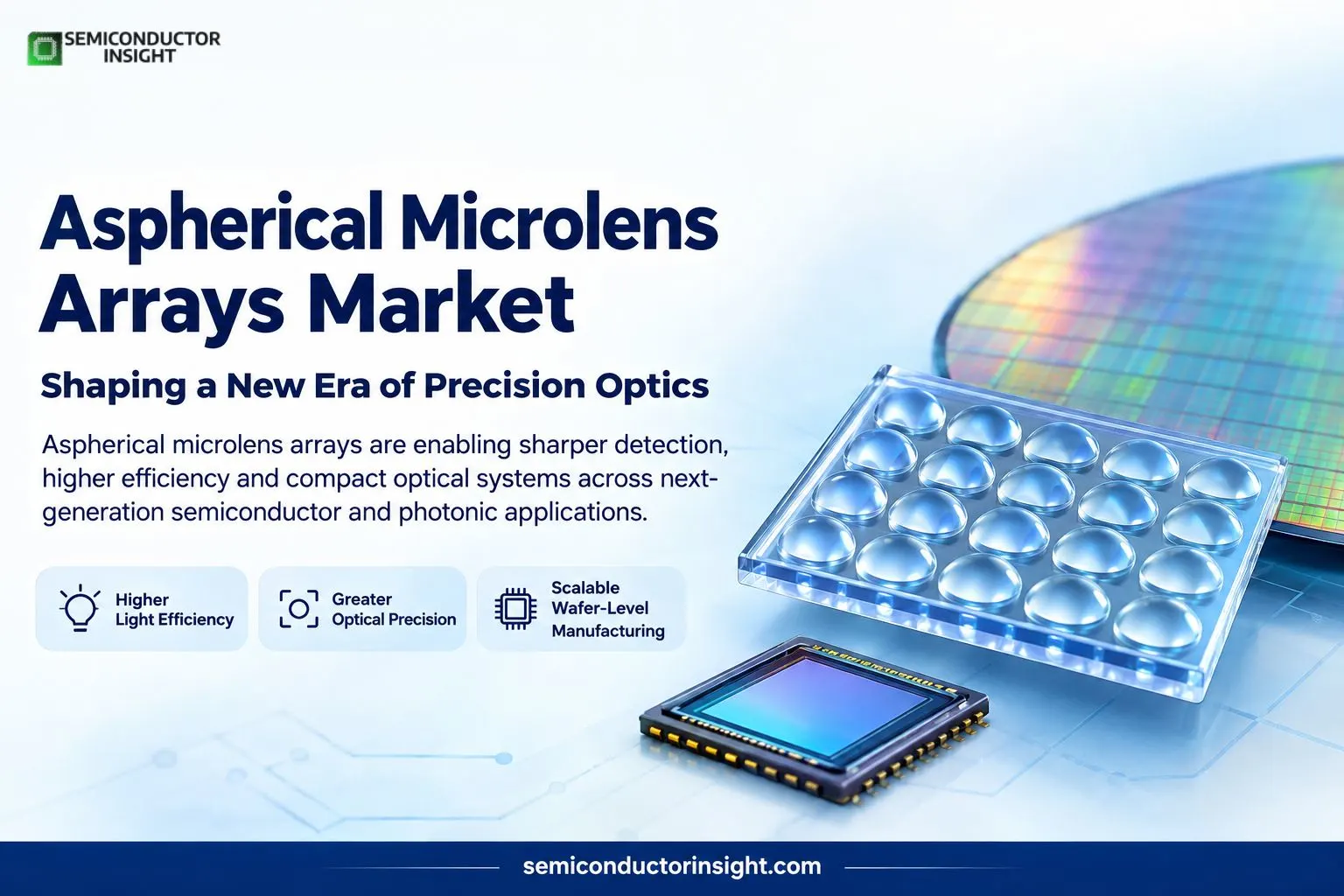
Aspherical Microlens Arrays Market 2026: From 5 μm Lens Features to 3,000 μm Optical Architectures
As semiconductor sensors become more compact, the optical structures placed above them are being engineered with much greater precision. Aspherical microlens arrays are part of this shift because their non-spherical surfaces can redirect, concentrate and shape incoming light more precisely than conventional spherical geometries.
Fraunhofer IOF reports microlens fabrication capabilities spanning approximately 5 μm to 3,000 μm lens diameters, with lens-gap resolution down to around 1 μm and focal-length homogeneity of approximately ±1% across a wafer. The same platform supports aspherical structures produced through reactive ion etching, alongside UV molding and other wafer-level processes.
That range matters because the same underlying micro-optical concept can be adapted for very different semiconductor architectures, from compact imaging sensors to detector arrays and laser-coupling systems.
Why the Aspherical Profile Matters?
A spherical lens does not always provide the optical correction required when the available space is extremely limited. An aspherical surface can be deliberately shaped to reduce optical aberrations and improve how photons reach the active sensing region.
This becomes particularly relevant when designers are trying to extract greater performance from increasingly small pixels.
Incoming photons → Aspherical surface → Controlled refraction → Reduced aberration → Higher usable signal
The technology therefore sits at an important intersection between semiconductor geometry and optical engineering. It is not simply a miniature version of a conventional camera lens.
A SPAD Example Shows the Performance Potential
- One of the clearest current examples comes from Fraunhofer IMS, where customized microlens arrays have been developed for SPAD sensors. The institute reports that integrating microlens arrays can increase the photon detection efficiency of its CSPAD αlpha platform by a factor of 7.
- The reason is closely connected to fill factor. SPAD pixels contain electronic circuitry that can occupy a substantial portion of the pixel area, limiting the physical region available for incoming photons. A properly designed microlens can redirect light toward the active detection area rather than allowing photons to fall onto inactive regions.
- This is particularly significant for applications where detecting very small quantities of light is more important than simply producing a conventional photographic image.
Wafer-Level Manufacturing Changes the Economics of Micro-Optics
The manufacturing story is becoming as important as the optical design itself. Fraunhofer IOF describes processes including grayscale lithography, binary-mask lithography with reflow, UV polymer molding, reactive ion etching and wafer-level integration with CMOS and VCSEL structures.
A research demonstration published through Nanomaterials showed the level of precision achievable through wafer-scale processing. Researchers fabricated a 50 mm-diameter wafer-level lens array containing 437 aspherical microlenses, each measuring 1 mm in diameter, with approximately 120 nm average-period moth-eye nanostructures. The antireflective nanostructures increased optical transmittance by roughly 3% across the 400–750 nm wavelength range.
You can freely browse our most recent updated related report to learn more about it before scrolling further: https://semiconductorinsight.com/report/aspherical-microlens-arrays-market/
The broader significance is the combination of optical precision and batch fabrication. Instead of manufacturing individual miniature lenses one by one, arrays can be patterned, replicated and assembled at wafer scale.
Smartphone Imaging Is Only One Piece of the Picture
CMOS image sensors remain a major environment for micro-optical integration. Sony’s development of stacked CMOS image sensors illustrates how aggressively semiconductor manufacturers are separating pixel and circuit functions to increase functionality within compact footprints. Sony states that its stacked architecture uses thousands of electrical connections between the pixel and circuit layers and was initially deployed in smartphone cameras.
As sensor architectures become more sophisticated, the optical layer must also be carefully matched to pixel geometry, incident angles and computational imaging requirements.
That opens applications beyond smartphones, including:
- Automotive sensing and imaging
- Machine vision
- Industrial inspection
- SPAD-based photon detection
- LiDAR architectures
- Security and surveillance
- Compact multi-aperture cameras
- VCSEL beam shaping and optical coupling
Fraunhofer IOF specifically identifies consumer electronics, automotive sensors, and machine vision and security systems among applications for wafer-level multi-aperture micro-optics.
A New Relationship with Silicon Photonics
Another important development is the increasing movement of optical technologies toward semiconductor-style wafer processing. In January 2025, imec demonstrated electrically driven GaAs nano-ridge lasers fabricated across 300 mm silicon wafers, achieving continuous-wave lasing at room temperature with threshold currents as low as 5 mA and optical output exceeding 1 mW.
Although laser integration and aspherical microlens arrays represent different technology layers, the manufacturing direction is similar: optical functionality is increasingly being designed around scalable semiconductor-compatible processes.
In December 2025, UMC also announced licensing of imec’s iSiPP300 silicon-photonics technology, including a 12-inch platform targeting next-generation connectivity.
The Micro-Optics Stack Is Becoming More Sophisticated
The next generation of optical semiconductor systems is increasingly built from multiple precisely engineered layers rather than a single lens.
Sensor / photonic device
↓
Optical isolation or aperture structure
↓
Aspherical microlens array
↓
Antireflective or nanostructured surface
↓
Wafer-level substrate
↓
CMOS or photonic semiconductor layer
This layered approach explains why aspherical microlens arrays are attracting attention across semiconductor research. Their value is not determined only by lens diameter. Surface profile, focal-length uniformity, optical crosstalk, wavelength response, alignment accuracy and wafer-level compatibility all influence the final system performance.
What Current Development Signals Are Revealing?
The strongest signal in 2026 is the convergence of micro-optics and semiconductor fabrication. Fraunhofer’s current work demonstrates wafer-level microlens integration directly on SPAD sensors, while its micro-optics platform supports lens structures from only a few micrometers to several millimeters.
At the same time, imec’s work on 300 mm silicon photonics, advanced optical interconnects and semiconductor-compatible optical devices shows how optical functions are increasingly being pulled closer to established wafer-processing ecosystems.
For Aspherical Microlens Arrays Market, this creates a particularly interesting development path. The technology is moving away from being viewed solely as a miniature imaging component and toward becoming an engineered optical layer within sophisticated semiconductor sensors, photonic devices and compact sensing platforms.

Comments (0)