Aspherical Microlens Arrays Market Insights
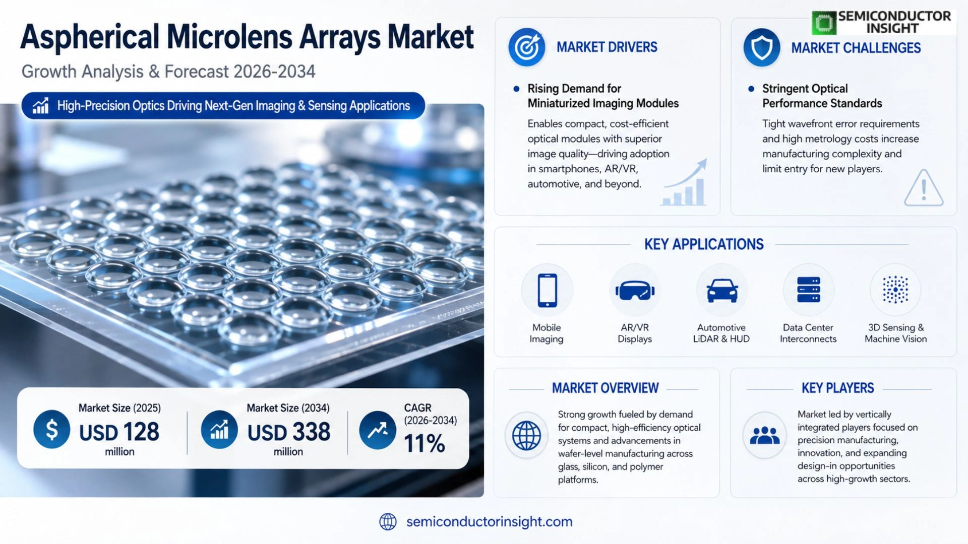
Aspherical Microlens Arrays market size was valued at USD 128 million in 2025. Forecasts indicate the market will reach approximately USD 338 million by 2034, reflecting an implied compound annual growth rate of about 11 % over the period.
Aspherical Microlens Arrays (AMAs) consist of one‑ or two‑dimensional arrays of micro‑scale lenslets whose surfaces follow an aspheric profile defined by a conic constant and higher‑order coefficients. This geometry corrects optical aberrations, improves numerical aperture and enhances coupling efficiency compared with conventional spherical microlenses, making AMAs suitable for high‑performance optical modules.
The upward trend stems from increasing demand for compact, low‑power optical subsystems in consumer electronics, automotive head‑up displays and data‑center interconnects. Because manufacturers seek fewer elements without sacrificing image quality, wafer‑level processing of glass, silicon or polymer substrates has become commonplace. At the same time, emerging applications such as AR/VR displays, lidar sensors and structured‑light imaging are expanding design‑in opportunities, prompting suppliers to invest in tighter tolerance control and vertical integration.
MARKET DRIVERS
Rising Demand for Miniaturized Imaging Modules
Aspherical Microlens Arrays market is gaining traction as smartphone manufacturers pursue thinner camera stacks. By correcting spherical aberrations without additional lens elements, aspherical microlens arrays enable smaller optical modules while preserving image sharpness. This efficiency directly cuts bill‑of‑materials costs, prompting OEMs to source higher volumes of these components.
Advances in Fabrication Techniques
Recent breakthroughs in grayscale lithography and UV‑curable polymer molding have lowered per‑unit production time. Vendors can now achieve sub‑micrometer surface tolerances at wafer‑scale yields, turning what was once a niche specialty into a mainstream supply. The resulting cost compression encourages adoption in automotive LiDAR and medical endoscopy, sectors where precision optics were previously prohibitive.
➤ “The convergence of compact system requirements and scalable manufacturing is reshaping the supply chain, turning aspherical microlens arrays into a commodity rather than a bespoke item.”
Beyond hardware, system integrators are bundling these arrays with AI‑driven image processing pipelines. The combined effect,higher optical performance plus software correction,creates a compelling value proposition for end‑users, accelerating market momentum.
MARKET CHALLENGES
Stringent Optical Performance Standards
Industries such as aerospace and defense impose exacting wavefront error limits. Even minor deviations in aspherical curvature can degrade sensor accuracy, forcing manufacturers to invest in additional metrology equipment. This capital intensity can deter smaller players from entering the market.
Other Challenges
Material Compatibility Issues
Certain high‑temperature polymer resins exhibit shrinkage that distorts the aspherical profile, limiting their use in harsh environments. Companies must either qualify new materials or redesign process windows, both of which extend time‑to‑market.
The need for rigorous qualification cycles also slows product rollout. Clients often request multiple prototype iterations to verify thermal stability, adding to development timelines and compressing margins.
MARKET RESTRAINTS
High Initial Capital Expenditure
Establishing a line capable of sub‑micron aspherical shaping requires clean‑room facilities, precision alignment rigs, and advanced inspection tools. The upfront outlay can exceed several million dollars, creating a financial barrier that favors established incumbents.
Moreover, the learning curve associated with new lithographic recipes means early‑stage production runs often suffer from yield variability. Investors therefore view the segment as higher risk compared with conventional spherical microlens suppliers.
MARKET OPPORTUNITIES
Emerging Applications in Augmented Reality
AR head‑up displays rely on compact optical stacks that can project high‑resolution imagery across a wide field of view. Aspherical microlens arrays meet this requirement by delivering uniform focus without bulky corrective elements. Early collaborations between lens manufacturers and AR chipset firms hint at a sizable revenue stream as the technology moves beyond prototyping.
Another promising frontier is quantum imaging, where wavefront precision directly influences entanglement fidelity. Suppliers that can certify nanometer‑scale surface accuracy stand to capture niche contracts from research institutions and defense laboratories.
Aspherical Microlens Arrays Market Trends
Compact Imaging Drives Design Innovation
The push toward smaller, power‑efficient cameras in smartphones, automotive sensors, and wearable devices is reshaping component specifications. Engineers favor microlens arrays that can correct aberrations within a reduced footprint, thereby eliminating one or two conventional glass elements. This substitution improves system reliability while keeping bill of materials low. Because the aspheric profile concentrates light more tightly, manufacturers can meet tighter performance envelopes without enlarging the optical stack. The ripple effect is a noticeable shift in product road‑maps: OEMs now request wafer‑level processed arrays that can be stacked directly onto image sensors, accelerating time‑to‑market for next‑generation vision modules.
Other Trends
Manufacturing Process Innovations
Recent advances in master‑mold replication and precision imprinting have raised yield levels above 90 % for polymer‑based substrates. Simultaneously, wafer‑scale etching on fused silica is achieving sub‑nanometer surface‑roughness, which translates into lower scatter loss for high‑NA applications. These process gains are not merely technical; they compress cycle times to weeks rather than months, allowing suppliers to respond swiftly to fluctuating demand from data‑center interconnects and AR/VR display makers. The competitive edge now hinges on the ability to lock down tighter process windows while maintaining margin profiles that range from the mid‑20s to the mid‑40s percent.
Vertical Integration and Supply‑Chain Consolidation
Customers with multi‑year design programmes are pressuring vendors to assume responsibility for design, tooling, wafer fabrication, and final assembly. This trend reduces hand‑off errors, improves thermal‑stability tracking, and delivers repeatable performance across production lots. Companies that have brought both the master‑tooling and coating steps in‑house report shorter iteration loops,often under 30 days,from prototype to pilot run. Moreover, the move toward hybrid optics, combining free‑form glass elements with polymer microlens arrays, is prompting a re‑evaluation of standard supply contracts, encouraging longer‑term partnership models rather than pure spot‑buy arrangements. The net result is a more resilient supply chain that can absorb material price volatility while delivering the high‑precision components demanded by optical‑communication modules and precision‑inspection equipment.
COMPETITIVE LANDSCAPE
Key Industry Players
Competitive Dynamics Shaping Aspherical Microlens Arrays market
Aspherical Microlens Arrays market is anchored by a handful of manufacturers that have built vertically integrated value chains, enabling them to control wafer‑level etching, master‑mold replication, and final assembly. INGENERIC, with its deep expertise in polymer‑on‑glass replication, commands roughly a quarter of global capacity and leverages a network of OEM relationships in data‑center interconnect and automotive optics. Its ability to sustain gross margins above 40 % stems from proprietary tooling and a disciplined yield‑management regime that minimizes scrap during dicing and coating. NIL Technology follows closely, differentiating itself through a hybrid silicon‑glass platform that delivers higher thermal stability for emerging AR/VR displays. Both firms have expanded into design services, shortening iteration cycles for customers who need custom freeform surfaces, and their market share reflects a broader trend toward consolidation around firms that can offer end‑to‑end optical solutions rather than discrete component supply.
Beyond the two dominant players, a constellation of niche specialists contributes depth to the competitive set. Axetris and SUMITA Optical Glass focus on high‑precision fused‑silica arrays for laser illumination, while AGC and Nippon Electric Glass (NEG) supply bulk glass substrates that feed both large‑volume and premium segments. Smaller but agile firms such as Holographix, Focuslight Technologies, and Power Photonic have carved out positions in the lidar and structured‑light sensing markets by offering rapid prototyping and low‑volume runs. Meanwhile, regional contributors,Shanghai Optics, temicon, and Viavi Solutions,provide localized support for Asian automotive suppliers and European telecom equipment makers, ensuring that the supply base remains diversified even as the industry moves toward tighter tolerances and higher reliability standards.
List of Key Aspherical Microlens Arrays Companies Profiled
- INGENERIC
- NIL Technology
- Axetris
- SUMITA Optical Glass
- AGC
- Nippon Electric Glass (NEG)
- Isuzu Glass
- Holographix
- Focuslight Technologies
- Power Photonic
- VIAVI Solutions
- Shanghai Optics
- temicon
- Nalux
Segment Analysis:
| Segment Category | Sub-Segments | Key Insights |
| By Type |
|
2D Aspherical Microlens Array
|
| By Application |
|
Data‑center Interconnect
|
| By End User |
|
Consumer Electronics
|
| By Lattice |
|
Hexagonal Lattice
|
| By Focal Length |
|
Chirped Focal Length
|
Regional Analysis: Aspherical Microlens Arrays Market
Europe
Automotive manufacturers are integrating aspherical microlens arrays into LIDAR modules to improve range accuracy while keeping form factors compact, prompting suppliers to tailor designs for mass‑production cycles.
Cross‑border university consortia receive EU funding to explore novel polymeric substrates, accelerating proof‑of‑concept projects that target next‑generation wearable optics.
Vertically integrated firms are consolidating wafer‑level processing with final optical assembly, reducing lead times and enhancing traceability for high‑value medical devices.
North America
North America continues to leverage its sizable consumer electronics ecosystem, where demand for high‑resolution display technologies fuels Aspherical Microlens Arrays market. Silicon Valley startups are experimenting with hybrid silicon‑polymer lenses that promise tighter focal spots for smartphone cameras, prompting incumbents to acquire niche players to broaden their product portfolios. Defense contractors also value the precision offered by aspherical microlens arrays for targeting optics, aligning procurement cycles with broader national security budgets. Though labor costs are comparable to Europe, the region’s emphasis on rapid prototyping and agile supply networks offsets price pressures, enabling manufacturers to experiment with low‑volume, high‑performance designs. Market participants are increasingly focusing on sustainability metrics, adopting greener manufacturing processes that align with corporate ESG commitments, thereby appealing to investors and environmentally conscious customers alike.
Asia‑Pacific
The Asia‑Pacific region presents a paradox of scale and specialization. While mass‑production capabilities in China and Taiwan enable cost‑effective fabrication of standard microlens arrays, Japan and South Korea excel in precision engineering for medical imaging and aerospace applications. Government initiatives in South Korea’s “Smart Factory” program encourage automation of wafer‑level processes, reducing defect rates and enhancing yield for aspherical geometries. Concurrently, Chinese manufacturers are expanding downstream capabilities, integrating microlens arrays into consumer wearables that target the burgeoning middle‑class market. The regional talent pool, rich in optical engineering expertise, supports a vibrant ecosystem of startups that experiment with metasurface‑based lens concepts, potentially reshaping the competitive landscape over the next decade.
South America
South America’s contribution to Aspherical Microlens Arrays market remains modest but is gaining traction through strategic investments in localized manufacturing. Brazil’s aerospace sector, bolstered by government subsidies, is exploring lightweight optical solutions for unmanned aerial vehicles, where aspherical microlens arrays can reduce system weight while preserving imaging fidelity. Emerging electronics assemblers in Chile and Argentina are establishing partnerships with European OEMs to assemble customized lens modules for regional medical device manufacturers. Although the market size is limited, the region’s focus on cost‑effective production and the willingness to adopt imported technologies suggest a gradual upward trajectory.
Middle East & Africa
In the Middle East & Africa, Aspherical Microlens Arrays market is driven primarily by defense and telecommunications projects. United Arab Emirates defense contractors are investing in high‑resolution surveillance optics that rely on aspherical microlens arrays to enhance detection capabilities in desert environments. Meanwhile, South Africa’s growing fintech sector is experimenting with biometric authentication devices that incorporate compact lens arrays to improve image capture under varied lighting conditions. Regional trade agreements are encouraging the import of specialized equipment, fostering a nascent supply chain that could mature as local expertise in micro‑optics deepens through academic collaborations.
Report Scope
This market research report provides a comprehensive analysis of the Aspherical Microlens Arrays Market , covering the forecast period 2026–2034. It offers detailed insights into market dynamics, technological advancements, competitive landscape, and key trends shaping the industry.
Key focus areas of the report include:
- Market Overview: The report begins with an overview outlining its current market scenario, key growth indicators, and industry transformation drivers. It discusses macroeconomic factors, demand–supply balance, regulatory landscape, and the strategic role of semiconductors in powering advancements across industries such as automotive, telecommunications, consumer electronics, and industrial automation.
- Market Size & Forecast: Historical data and future projections for revenue, unit shipments, and market value across major regions and segments.
- Segmentation Analysis: Detailed breakdown by product type, technology, application, and end-user industry to identify high-growth segments and investment opportunities.
- Regional Insights: Insights into market performance across North America, Europe, Asia-Pacific, Latin America, and the Middle East & Africa, including country-level analysis where relevant.
- Competitive Landscape: Profiles of leading market participants, including their product offerings, R&D focus, manufacturing capacity, pricing strategies, and recent developments such as mergers, acquisitions, and partnerships.
- Technology Trends & Innovation: Assessment of emerging technologies, integration of AI/IoT, semiconductor design trends, fabrication techniques, and evolving industry standards.
- Market Drivers & Restraints: Evaluation of factors driving market growth along with challenges, supply chain constraints, regulatory issues, and market-entry barriers.
- Stakeholder Insights: Insights for component suppliers, OEMs, system integrators, investors, and policymakers regarding the evolving ecosystem and strategic opportunities.
Primary and secondary research methods are employed, including interviews with industry experts, data from verified sources, and real-time market intelligence to ensure the accuracy and reliability of the insights presented.
FREQUENTLY ASKED QUESTIONS:
What is the current market size of Aspherical Microlens Arrays Market?
-> Aspherical Microlens Arrays market forecasts indicate the market will reach approximately USD 338 million by 2034, reflecting an implied CAGR of about 11 %
Which key companies operate in Aspherical Microlens Arrays Market?
-> Key players include INGENERIC, NIL Technology, Axetris, SUMITA Optical Glass, AGC, Nippon Electric Glass (NEG), Isuzu Glass, Holographix, Focuslight Technologies, Power Photonic, Nalux, VIAVI Solutions, Shanghai Optics, temicon.
What are the key growth drivers?
-> Key growth drivers include the increasing demand for compact, low‑power optical modules in consumer and in‑vehicle applications, rising data‑center interconnect and precision‑inspection requirements, and the expansion of AR/VR, lidar and structured‑light sensing systems.
Which region dominates the market?
-> Asia accounts for the largest share of the market, driven by strong manufacturing bases and growing adoption in electronics and automotive sectors.
What are the emerging trends?
-> Emerging trends include integration of freeform and hybrid optics, reflow‑compatible packaging, and the deployment of Aspherical Microlens Arrays in AR/VR displays, lidar and advanced imaging solutions.

Get Sample Report PDF for Exclusive Insights
Report Sample Includes
- Table of Contents
- List of Tables & Figures
- Charts, Research Methodology, and more...