

Aluminum vs. Copper Insulated Metal Substrates 2026: Where Each Material Makes Sense
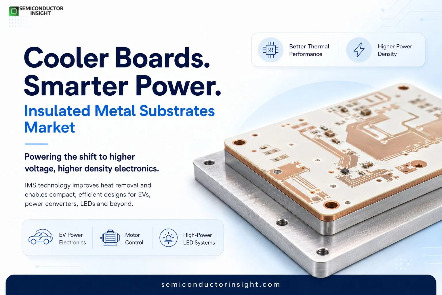
As semiconductor devices become smaller and power electronics pack more switching capability into tighter spaces, thermal management is moving closer to the center of PCB engineering. This is where Insulated Metal Substrates Market becomes particularly relevant. An insulated metal substrate, commonly called IMS, replaces the conventional PCB structure with a metal carrier, an electrically insulating but thermally conductive dielectric layer, and a copper circuit layer.
The concept is straightforward: move heat away from the active device more efficiently while retaining the electrical insulation needed for the circuit. Würth Elektronik describes IMS boards as a solution for applications such as LED systems, motor control and current conversion, where conventional FR4-based structures can face greater thermal-management demands.
You Can Freely Surf Our Latest Updated Report Here: https://semiconductorinsight.com/report/insulated-metal-substrates-market/
The Three-Layer Architecture behind the Technology
Power-generating component → Copper circuit → Thermal dielectric → Metal carrier → Heat sink or chassis
- Aluminum is commonly selected as the carrier because it combines relatively low weight with useful heat-spreading capability, although copper and stainless steel are also used for specific designs.
- IPC documentation describes IMS constructions using aluminum base layers of approximately 1, 1.5, 2 or 3 mm, while copper circuit layers can range from 35 to 105 μm in the referenced configurations.
- The dielectric is particularly important. Würth notes that thermally optimized insulation materials can achieve thermal conductivity up to 5 times that of conventional prepreg, helping reduce the thermal barrier between the copper circuitry and metal carrier.
Why 800 V Electronics Are Changing the Conversation
Electric-vehicle power electronics provide one of the clearest examples of why thermal design is becoming more demanding. Modern onboard chargers and DC/DC converters are being designed around higher voltage and power-density requirements, with silicon-carbide devices enabling faster switching and compact converter architectures.
A Würth Elektronik reference design using Wolfspeed SiC MOSFETs demonstrates a 22 kW bidirectional CLLC converter using an IMS board. The design operates across a 200-800 V DC battery range, switches at 135-250 kHz, reaches a reported 9.4 kW/L power density and achieves more than 98.6% peak efficiency.
Those figures illustrate why the substrate cannot be treated as a passive piece of the electronics assembly. At high power density, the path between a semiconductor junction and the cooling system directly affects the usable operating envelope.
LEDs Were Early Adopters, Power Electronics Are Expanding the Use Case
- IMS technology has long been associated with high-power LED boards because LEDs convert part of their electrical input into heat that must be removed continuously. The same basic thermal principle now applies across motor controllers, power converters, automotive electronics and other high-current systems.
- The attraction is packaging efficiency. Instead of mounting a conventional PCB onto a separate heat-spreading structure, an IMS design integrates the metal thermal path directly into the board construction.
- This can reduce the number of interfaces between the heat-producing component and the cooling structure, although the actual advantage depends heavily on board construction, component layout, dielectric properties and cooling architecture.
A 2025 Research Result Shows Why Substrate Selection Matters
Recent research also demonstrates that IMS is not automatically the best answer for every high-power application. Oak Ridge National Laboratory researchers compared five substrate technologies for space-constrained power modules, including conventional IMS, direct-bonded copper, direct-bonded aluminum, double-sided cooling and a pyrolytic-graphite-enhanced IMS approach.
Their work is revealing because it treats substrate selection as a thermal-engineering decision rather than a simple material substitution. The proposed modified DBC architecture achieved 20% greater loss-handling capability than an identical DBC configuration in experimental validation.
For IMS developers, this reinforces an important point: the next stage of innovation will not simply be about adding more thermally conductive material. It will involve optimizing the entire heat path.
From Metal Core to Smarter Thermal Architecture
The next wave of IMS development is moving toward higher-conductivity dielectric systems, improved copper configurations and alternative metal carriers. Aluminum remains attractive for weight-sensitive designs, while copper can provide stronger thermal performance where mass and cost are acceptable.
There is also growing interest in integrating advanced thermal materials into substrate structures. The 2025 ORNL study specifically examined a thermally annealed pyrolytic-graphite-based IMS, showing how research is moving beyond conventional aluminum-core construction.
Where IMS Fits in the New Semiconductor Hardware Stack
Si / SiC device
↓
Power package
↓
Copper circuit layer
↓
Thermally conductive dielectric
↓
Aluminum or copper carrier
↓
Heat sink / chassis
↓
Ambient cooling
That architecture is particularly relevant as semiconductor switching speeds increase and automotive, industrial and energy-conversion systems become more compact.
The Real Market Story Is About Watts per Liter
The most useful way to understand Insulated Metal Substrates Market is not simply by counting boards. It is by looking at how much electrical functionality engineers are trying to place into a limited physical volume.
The 22 kW, 9.4 kW/L reference design is a useful illustration of this trend. As power density rises, thermal paths become shorter, more deliberate and increasingly integrated into the PCB itself.
That is giving IMS technology a stronger position in applications where heat, electrical insulation, compact packaging and mechanical integration must work together. The market’s evolution is therefore closely tied to a broader semiconductor hardware shift: electronics are becoming smaller, faster and more powerful, while the available space for removing heat is becoming increasingly limited.

Comments (0)