
AI Workload Surge Powering Advanced Packaging for AI Chip Market
The rapid expansion of artificial intelligence workloads is fundamentally transforming semiconductor design, pushing advanced packaging technologies to the forefront of innovation. AI processors, in contrast to conventional chips, need very high bandwidth, low latency, and effective power distribution. Because of this change, packaging is now a vital performance enabler rather than a backend procedure.
Advanced packaging techniques such as 2.5D interposers, 3D stacking, and chiplet integration are now central to AI chip development. These approaches allow multiple dies to be integrated into a single package, significantly improving computational density. For example, AI accelerators used in large-scale training models often integrate high-bandwidth memory (HBM) stacks directly with processing units, reducing data transfer bottlenecks.
The growing complexity of AI models, particularly large language models and generative AI systems, has increased the need for packaging solutions that can handle massive data flows while maintaining thermal stability.
Engineering Precision through Heterogeneous Integration
- One of the defining characteristics of advanced packaging in AI chips is heterogeneous integration. This involves combining logic, memory, and specialized accelerators within a single package to optimize performance. It allows chip designers to bypass the limitations of monolithic scaling while maintaining flexibility in design.
- Recent industry implementations demonstrate this trend. AI chips deployed in hyperscale data centers often include multiple chiplets interconnected through silicon bridges or advanced substrates. These configurations enable faster communication speeds compared to traditional board-level connections.
- From a technical standpoint, interconnect density in advanced packaging has reached levels exceeding 10,000 connections per square millimeter in high-end designs, enabling unprecedented data exchange rates within compact architectures. This capability is critical for AI inference and training applications that demand real-time processing.
Thermal Management as a Design Differentiator
As AI chips become more powerful, heat generation has emerged as a major constraint. Advanced packaging is playing a crucial role in addressing thermal challenges through innovative cooling and material solutions.
Technologies such as embedded heat spreaders, microfluidic cooling channels, and advanced thermal interface materials are being integrated directly into chip packages. This ensures efficient heat dissipation even under high computational loads.
In high-performance AI accelerators, power densities have surpassed 1,000 watts per square centimeter in localized hotspots, necessitating advanced thermal strategies. Without effective packaging solutions, maintaining operational stability in such environments would be extremely difficult.
The focus on thermal efficiency is not only improving chip reliability but also enabling sustained performance in data-intensive AI workloads.
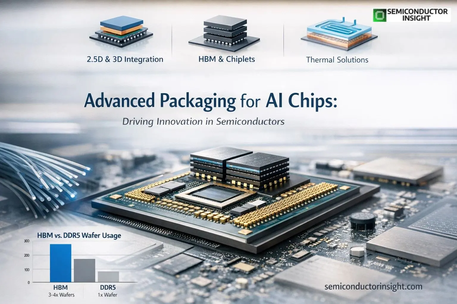
HBM production intensity vs. standard DRAM
The entire DRAM supply chain is altered because 1 GB of HBM requires 3 – 4× more wafer capacity to produce than 1 GB of DDR5.
- HBM (1 GB): 3 – 4× wafers
- DDR5 (1 GB): 1× baseline
- HBM revenue share: >30% DRAM
- HBM output share: ~8% bits
Supply Chain Realignment around Advanced Packaging Ecosystems
The growing importance of advanced packaging has led to a significant restructuring of the semiconductor supply chain. Foundries, outsourced semiconductor assembly and test providers (OSATs), and substrate manufacturers are increasingly collaborating to deliver integrated solutions.
Major semiconductor manufacturers are investing heavily in packaging capabilities, moving beyond traditional outsourcing models. This vertical integration is aimed at ensuring better control over performance optimization and production timelines.
Additionally, substrate demand has intensified, particularly for high-density organic and silicon interposer-based solutions. Industry reports indicate that advanced substrate production lines are operating at near-full capacity in leading manufacturing hubs, reflecting strong demand from AI chip producers.
To Know More about the Report, You Can Freely Browse Our Latest Updated Report: https://semiconductorinsight.com/report/advanced-packaging-for-ai-chip-market/
Regional Leadership Shaping Technology Advancement
- Asia Pacific stands as the dominant hub for advanced packaging innovation, particularly due to its strong manufacturing ecosystem. Countries like Taiwan and South Korea lead in both technology development and large-scale production. Taiwan alone accounts for a significant share of global advanced packaging capacity, supported by leading semiconductor foundries and OSAT providers.
- The region’s strength lies in its integrated supply chain, advanced infrastructure, and continuous investment in research and development. Fabrication facilities in this region handle a substantial portion of global AI chip packaging, with production volumes reaching millions of units annually for high-performance applications.
- North America, on the other hand, is emerging as a critical center for design innovation and strategic investment. The United States has increased funding for semiconductor manufacturing and packaging through government initiatives such as the CHIPS Act. Recent allocations include billions of dollars directed toward advanced packaging research and domestic manufacturing capabilities.
- Additionally, leading technology companies in North America are driving innovation by developing proprietary packaging technologies tailored for AI workloads. This combination of policy support and corporate investment is strengthening the region’s position in the global ecosystem.
Material Innovation and Process Advancements
Material science is playing a pivotal role in advancing packaging technologies. The shift toward finer interconnects and higher integration densities requires new materials with superior electrical and thermal properties.
Advanced substrates, low-loss dielectrics, and high-performance bonding materials are being developed to meet these requirements. For example, hybrid bonding techniques are enabling direct copper-to-copper connections between dies, significantly improving signal integrity and reducing latency.
Process innovations such as wafer-level packaging and panel-level packaging are also gaining traction, offering scalability and cost efficiency for high-volume production.
These advancements are not only enhancing performance but also enabling the integration of more complex AI functionalities within compact form factors.

Comments (0)