
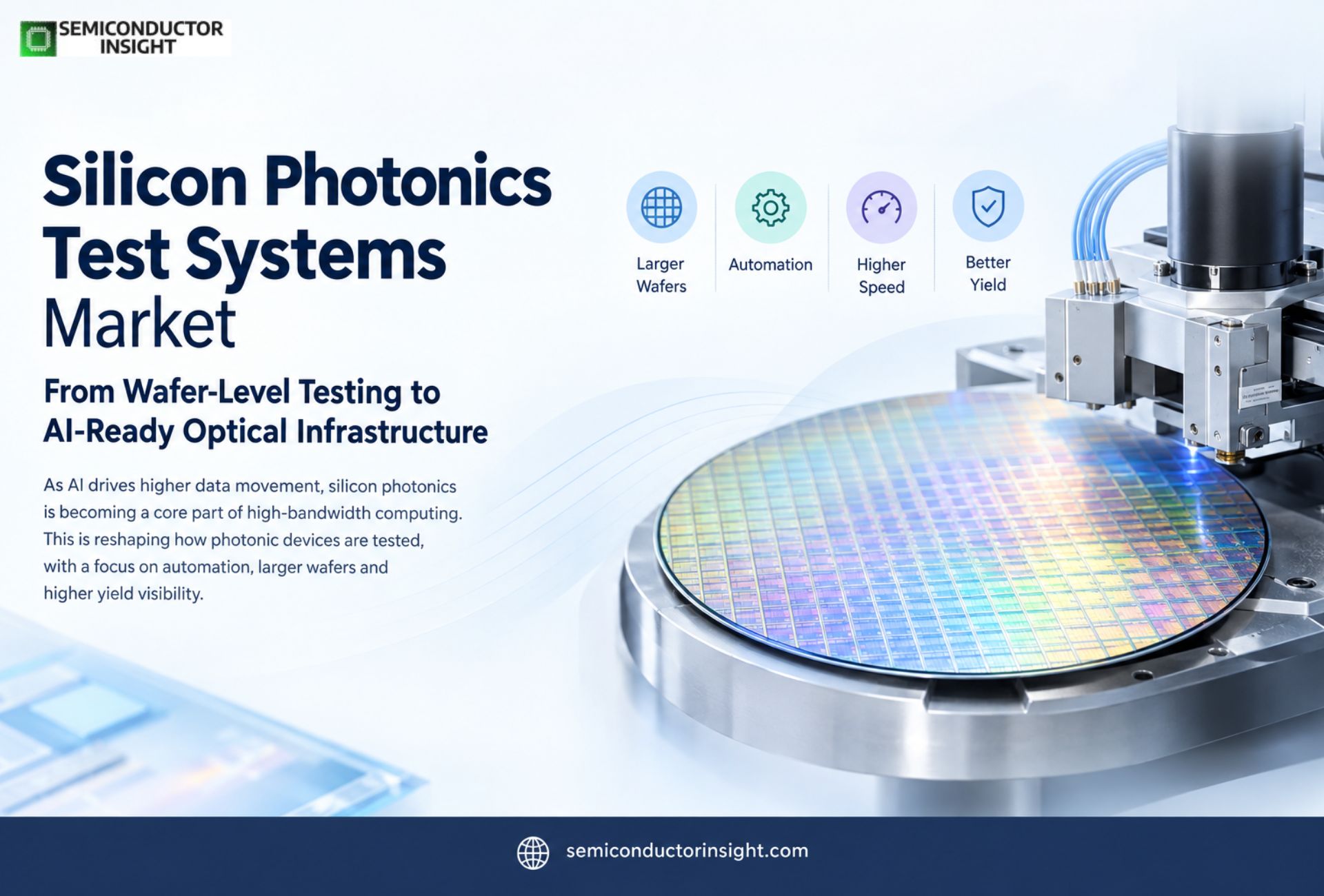
AI Data Center Expansion Puts Wafer-level Silicon Photonic Test Systems at the Center of Optical Manufacturing
Silicon photonics is moving from a specialized optical technology toward a manufacturing platform for high-bandwidth computing infrastructure. As AI systems push data movement between processors, memory and networking equipment, optical interconnects are becoming increasingly important. That shift is changing the role of testing.
- Instead of waiting until individual photonic dies or packaged devices are available, manufacturers are increasingly looking at wafer-level characterization, automated optical coupling and wafer-level burn-in.
- The objective is straightforward: identify defective photonic devices earlier, improve yield visibility and create known-good photonic components before expensive downstream assembly.
300 mm Is Becoming a Defining Specification
The move toward larger wafers is one of the most visible changes in photonic testing.
A 300 mm wafer provides substantially more die positions than smaller formats, making automated probing and optical alignment increasingly important for production environments. FormFactor now offers a dedicated 300 mm silicon photonics probing platform supporting wafer and die-level measurements, automated calibration and both vertical and edge optical coupling.
The development is not limited to conventional single-sided probing. MPI’s TS3000-DS platform is designed for double-sided 300 mm silicon photonics testing, allowing electrical contact from one side while optical fiber arrays are aligned from the opposite side. This architecture is particularly relevant to advanced photonic packaging approaches.
You Can Go Through Our Latest Updated Insights Here: https://semiconductorinsight.com/report/wafer-level-silicon-photonic-test-system-market/
AI Infrastructure Is Changing What Test Systems Must Measure
- AI clusters are increasing the amount of information that must move between computing components. This is creating a stronger requirement for optical technologies capable of supporting high-speed links while maintaining manufacturing consistency.
- Intel’s current silicon photonics portfolio includes 400 Gb/s, 800 Gb/s and 1.6 Tb/s solutions. Its platform also integrates laser technology at wafer scale, connecting manufacturing and testing more closely with optical transceiver production.
- For test-system manufacturers, this translates into higher-speed electrical characterization, optical power measurements, wavelength verification, coupling optimization and automated data collection rather than basic pass/fail inspection.
Automation Is Becoming Part of the Measurement Architecture
Modern photonic wafer testing is increasingly combining the probe station, optical alignment hardware, measurement instruments and software into a single automated workflow.
- FormFactor’s silicon photonics platform uses machine vision, automated optical calibration and software-controlled alignment. Its published testing results demonstrate coupled-power repeatability across 900 measurements with variation below 0.3 dB.
- A March 2025 release from ficonTEC introduced a 300 mm double-sided electro-optical wafer tester with automated wafer loading, six-axis optical alignment, fiber-array calibration, end-face inspection and automated photonic integrated circuit mapping.
This illustrates an important change in test architecture. Automation is no longer simply being added to reduce operator involvement. It is being used to make optical measurements more repeatable across large wafer populations.
Wafer-level Burn-in Moves into the AI Optical Pipeline
Testing does not stop with optical characterization. Reliability screening is becoming another important application.
- In March 2026, Aehr Test Systems announced a follow-on order for an automated wafer-level test and burn-in system from a silicon photonics customer serving data-center optical interconnect applications. The system included 300 mm automation.
Aehr subsequently announced another production order in June 2026 for a system configured to test nine wafers in parallel for a major networking customer developing silicon photonics transceivers and optical I/O products for hyperscale AI and cloud data centers.
- In July 2026, another Aehr announcement described a fully automated system supporting high-volume production burn-in of silicon photonics devices for AI optical interconnect and hyperscale data-center applications, with up to nine 300 mm wafers tested in parallel.
India Is Building the Characterization Layer
The development is also visible in research infrastructure outside the largest commercial photonics manufacturers.
The Centre for Programmable Photonic Integrated Circuits and Systems at IIT Madras operates a silicon photonics testing and characterization facility supporting electrical, optical and electro-optical measurements up to 50 GHz. Its infrastructure includes 8-inch wafer probe stations and equipment for grating-coupled and edge-coupled photonic devices.
This type of facility matters because wafer-level testing is increasingly relevant not only to mass production but also to process development, device validation and photonic integrated circuit research.
From Optical Measurement to Manufacturing Intelligence
The next phase of wafer-level silicon photonic testing is increasingly about the data generated during measurement.
A production system can potentially connect optical coupling results, electrical characteristics, wafer coordinates, temperature conditions and device-level performance into a single dataset. That creates a clearer link between test results and manufacturing yield.
Recent patent activity also reflects this direction. A silicon photonic wafer testing system disclosed in a 2026 U.S. patent application integrates wafer probing, optical coupling, optical measurement, cameras and centralized control to establish positional relationships between probes, fiber arrays and photonic couplers.
For manufacturers, that convergence could make wafer testing less of a final inspection step and more of a real-time manufacturing intelligence layer.
Why the 2026 Test Architecture Looks Different?
The strongest change is not simply the movement from 200 mm to 300 mm wafers. It is the combination of larger wafers, optical automation, high-speed electrical measurement, software-controlled alignment, parallel testing and reliability screening.
FIBERPRO, for example, describes a silicon photonics wafer tester capable of supporting wafers up to 12 inches depending on the probe station, with automatic optical coupling, image-processing alignment and automatic height control.
As AI optical I/O, co-packaged optics and high-speed data-center connectivity continue moving into production, the test system increasingly becomes part of the photonics manufacturing platform itself.

Comments (0)