Key Statistics
Key Takeaways
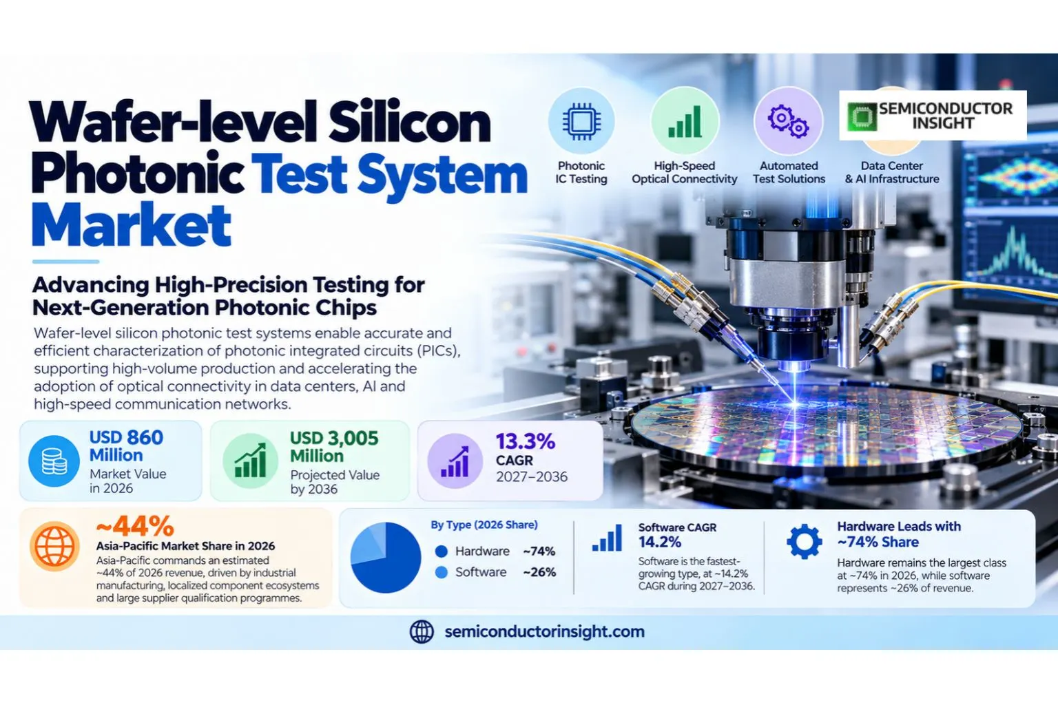
- Market trajectory: The wafer-level silicon photonic test system market stands at USD 860 million in 2026 and is projected to reach USD 3,005 million by 2036, a 13.3% CAGR during 2027–2036. Demand reflects 1.6T interconnect migration and co-packaged optical packaging, with buyers increasingly insisting on optical alignment, wavelength-swept characterization, electro-optical probing and automated wafer mapping that support measurable performance and cost control.
- Hardware lead: An estimated ~74% of base-year revenue is assigned to Hardware, while Software carries an estimated ~14.2% CAGR and ~26% share. The technological transition matters for procurement because buyers must weigh productivity and serviceability against the qualification effort associated with a new technical platform.
- 300mm Wafer application: The leading application accounts for an estimated ~56% share, with 300mm Wafer representing the fastest estimated application growth at ~14.1% CAGR. Requirements differ between high-volume and specialist users, especially where an upgraded optical interface changes both the delivered product specification and the cost of field support.
- Asia-Pacific leadership: The region captures an estimated ~44% of 2026 revenue; Asia-Pacific is the fastest-growing geography at ~14.1% CAGR. Factory concentration, engineering capabilities and customer procurement determine the local purchasing routes, while countries with limited manufacturing infrastructure depend more heavily on imported specialist systems.
- Principal restraint: micron-scale fiber coupling alignment and low test throughput can impede adoption even when underlying demand increases. In 2026 procurement reviews increasingly prioritize verifiable supplier claims, thermal and environmental stability, warranty coverage and repeatable production outcomes. A lower quoted system price may not compensate for process downtime or reduced useful life.
Wafer-level Silicon Photonic Test System Market Overview
Wafer-level silicon photonic test system market was valued at USD 860 million in 2026 and is projected to reach USD 3,005 million by 2036, representing a CAGR of 13.3% over 2027–2036. Asia-Pacific commands an estimated ~44% of 2026 revenue, reflecting industrial manufacturing, localized component ecosystems and large supplier qualification programmes.
Wafer-level Silicon Photonic Test System describes the commercial equipment, optical assembly and application-specific engineering sold to silicon-photonics foundries, photonic integrated circuit design houses and outsourced test-and-assembly specialists. The economic unit is recognized revenue for in-scope hardware and associated software, not the gross sales of downstream data centers or finished end-user platforms. Suppliers compete on technical qualification and lifecycle cost rather than a simple count of end products. Automated optical and electro-optical equipment, software, stages and measurement cells sold for wafer-level silicon photonic device characterization; excludes fabrication lithography, finished transceivers and stand-alone long-haul networking equipment.
The 2026 market boundary requires careful separation from adjacent products. Automated optical and electro-optical equipment, software, stages and measurement cells sold for wafer-level silicon photonic device characterization; excludes fabrication lithography, finished transceivers and stand-alone long-haul networking equipment. Components embedded in a complete customer platform enter the boundary only at the relevant module or equipment selling value, avoiding a false comparison with customer-wide spending that includes unrelated electronics and service content.
Technical differentiation centres on optical alignment, wavelength-swept characterization, electro-optical probing and automated wafer mapping. Unlike conventional DC wafer probing, a photonic test station aligns one or more optical fibres to sub-micron waveguide interfaces, controls wavelength and polarization, and synchronizes electrical bias with optical readout. Fixture drift, vibration, thermal movement and optical coupling loss create significant sources of uncertainty, so automation value depends on the reproducibility of alignment as much as raw scanning speed. In qualification meetings, buyers verify tolerances against a real device configuration rather than taking an ideal laboratory specification as proof of manufacturing repeatability.
Capital spending and product demand generate purchase orders differently in this industry. A foundry purchases a production-ready station when its photonic process-control monitors or known-good-die qualification move beyond engineering runs. In research laboratories, smaller stations are sold with tunable lasers, polarization controllers, power meters and piezo stages; on 300mm lines, a supplier must demonstrate automatic calibration, throughput and traceable wafer mapping before obtaining equipment acceptance. Among visible 2025–2026 signals, FormFactor demonstrated a TRITON integrated silicon-photonics test cell in March 2026 that unifies alignment and measurement. That event demonstrates the link between technical acceptance and subsequent equipment or module procurement.
The competitive cycle is changing because of 1.6T interconnect migration and co-packaged optical packaging, yet volume does not rise uniformly across technology classes or countries. Keysight specifies tunable lasers, polarization control, power meters and source-measurement units as synchronized photonic functional test elements. In 2027–2036, suppliers that shorten testing or qualification time while protecting lifetime reliability can capture demand even when average realized prices soften.
Segment Analysis: By Type
The type split covers Software, Hardware. Hardware remains the largest class at an estimated ~74% in 2026, while Software grows fastest at ~14.2% CAGR and represents ~26% of revenue. Unlike conventional DC wafer probing, a photonic test station aligns one or more optical fibres to sub-micron waveguide interfaces, controls wavelength and polarization, and synchronizes electrical bias with optical readout. Fixture drift, vibration, thermal movement and optical coupling loss create significant sources of uncertainty, so automation value depends on the reproducibility of alignment as much as raw scanning speed.
| Type | Function | Market position |
|---|---|---|
| Software | Software addresses a specific part of optical alignment, wavelength-swept characterization, electro-optical probing and automated wafer mapping. Its practical function is assessed through performance, interface compatibility, production process requirements and the underlying buyer application. Unlike conventional DC wafer probing, a photonic test station aligns one or more optical fibres to sub-micron waveguide interfaces, controls wavelength and polarization, and synchronizes electrical bias with optical readout. Fixture drift, vibration, thermal movement and optical coupling loss create significant sources of uncertainty, so automation value depends on the reproducibility of alignment as much as raw scanning speed. For the Software class, acceptance trials must reflect the operating environment instead of relying on marketing specifications alone. | Type segment: an estimated ~26% of 2026 revenue, ~14.2% CAGR. FormFactor demonstrated a TRITON integrated silicon-photonics test cell in March 2026 that unifies alignment and measurement. Software purchasing decisions are shaped by product-generation transitions and whether supply contracts can support stable service, measurement or assembly tolerances. A segment may add unit shipments without matching revenue gains when intense competition pushes down its realized selling price. For wafer-level silicon photonic test system, the commercial implication is that the customer must balance measurable performance, service support and repeatability before committing the next production or deployment programme. A cheaper device cannot substitute for qualified output when failure would disrupt later stages of a multi-step product build. |
| Hardware | Hardware addresses a specific part of optical alignment, wavelength-swept characterization, electro-optical probing and automated wafer mapping. Its practical function is assessed through performance, interface compatibility, production process requirements and the underlying buyer application. Unlike conventional DC wafer probing, a photonic test station aligns one or more optical fibres to sub-micron waveguide interfaces, controls wavelength and polarization, and synchronizes electrical bias with optical readout. Fixture drift, vibration, thermal movement and optical coupling loss create significant sources of uncertainty, so automation value depends on the reproducibility of alignment as much as raw scanning speed. For the Hardware class, acceptance trials must reflect the operating environment instead of relying on marketing specifications alone. | Largest type: an estimated ~74% of 2026 revenue, ~13.0% CAGR. Keysight specifies tunable lasers, polarization control, power meters and source-measurement units as synchronized photonic functional test elements. Hardware purchasing decisions are shaped by product-generation transitions and whether supply contracts can support stable service, measurement or assembly tolerances. A segment may add unit shipments without matching revenue gains when intense competition pushes down its realized selling price. For wafer-level silicon photonic test system, the commercial implication is that the customer must balance measurable performance, service support and repeatability before committing the next production or deployment programme. A cheaper device cannot substitute for qualified output when failure would disrupt later stages of a multi-step product build. |
Segment Analysis: By Application
By application, the segmentation comprises 300mm Wafer, 200mm Wafer, 150mm Wafer, Others. 300mm Wafer represents the leading demand category at an estimated ~56% share, while 300mm Wafer advances at ~14.1% CAGR. A foundry purchases a production-ready station when its photonic process-control monitors or known-good-die qualification move beyond engineering runs. In research laboratories, smaller stations are sold with tunable lasers, polarization controllers, power meters and piezo stages; on 300mm lines, a supplier must demonstrate automatic calibration, throughput and traceable wafer mapping before obtaining equipment acceptance.
| Application | Demand characteristics |
|---|---|
| 300mm Wafer | 2026 application share estimated at ~56%, with ~14.1% CAGR. The 300mm Wafer category creates demand when silicon-photonics foundries, photonic integrated circuit design houses and outsourced test-and-assembly specialists require a validated implementation for this use case. A foundry purchases a production-ready station when its photonic process-control monitors or known-good-die qualification move beyond engineering runs. In research laboratories, smaller stations are sold with tunable lasers, polarization controllers, power meters and piezo stages; on 300mm lines, a supplier must demonstrate automatic calibration, throughput and traceable wafer mapping before obtaining equipment acceptance. The final specification therefore depends on application intensity and repeatability, rather than a uniform procurement list for every customer class. |
| 200mm Wafer | 2026 application share estimated at ~29%, with ~12.6% CAGR. The 200mm Wafer category creates demand when silicon-photonics foundries, photonic integrated circuit design houses and outsourced test-and-assembly specialists require a validated implementation for this use case. A foundry purchases a production-ready station when its photonic process-control monitors or known-good-die qualification move beyond engineering runs. In research laboratories, smaller stations are sold with tunable lasers, polarization controllers, power meters and piezo stages; on 300mm lines, a supplier must demonstrate automatic calibration, throughput and traceable wafer mapping before obtaining equipment acceptance. The final specification therefore depends on application intensity and repeatability, rather than a uniform procurement list for every customer class. |
| 150mm Wafer | 2026 application share estimated at ~11%, with ~10.8% CAGR. The 150mm Wafer category creates demand when silicon-photonics foundries, photonic integrated circuit design houses and outsourced test-and-assembly specialists require a validated implementation for this use case. A foundry purchases a production-ready station when its photonic process-control monitors or known-good-die qualification move beyond engineering runs. In research laboratories, smaller stations are sold with tunable lasers, polarization controllers, power meters and piezo stages; on 300mm lines, a supplier must demonstrate automatic calibration, throughput and traceable wafer mapping before obtaining equipment acceptance. The final specification therefore depends on application intensity and repeatability, rather than a uniform procurement list for every customer class. |
| Others | 2026 application share estimated at ~4%, with ~12.9% CAGR. The Others category creates demand when silicon-photonics foundries, photonic integrated circuit design houses and outsourced test-and-assembly specialists require a validated implementation for this use case. A foundry purchases a production-ready station when its photonic process-control monitors or known-good-die qualification move beyond engineering runs. In research laboratories, smaller stations are sold with tunable lasers, polarization controllers, power meters and piezo stages; on 300mm lines, a supplier must demonstrate automatic calibration, throughput and traceable wafer mapping before obtaining equipment acceptance. The final specification therefore depends on application intensity and repeatability, rather than a uniform procurement list for every customer class. |
Distribution channels influence how orders are won in wafer-level silicon photonic test system. Direct OEM qualification is typically necessary when the module or system forms part of a mission-critical product, while system integrators and specialist distributors serve laboratory, replacement and regional small-order requirements. micron-scale fiber coupling alignment and low test throughput makes pre-sales validation and post-installation engineering material elements of supplier selection. For wafer-level silicon photonic test system, the commercial implication is that the customer must balance measurable performance, service support and repeatability before committing the next production or deployment programme. A cheaper device cannot substitute for qualified output when failure would disrupt later stages of a multi-step product build.
Regional Analysis
Asia-Pacific holds the largest estimated 2026 share at ~44%, followed by North America at ~25% and Europe at ~20%. Asia-Pacific has the highest forecast growth at about ~14.1% CAGR. Large East Asian manufacturing networks shorten access to precision optics, process-control engineering and high-volume assembly. China, Japan, South Korea and India differ in their capacity to manufacture a complete system, so qualified products frequently travel across borders before final deployment. The regional purchasing decision weighs warranty coverage and replacement-part availability alongside technical performance. For wafer-level silicon photonic test system, the commercial implication is that the customer must balance measurable performance, service support and repeatability before committing the next production or deployment programme. A cheaper device cannot substitute for qualified output when failure would disrupt later stages of a multi-step product build.
How do manufacturing, commercialization and procurement differ among the five wafer-level silicon photonic test system regions?
The five regional markets operate under distinct procurement patterns. Large East Asian manufacturing networks shorten access to precision optics, process-control engineering and high-volume assembly. China, Japan, South Korea and India differ in their capacity to manufacture a complete system, so qualified products frequently travel across borders before final deployment. The regional purchasing decision weighs warranty coverage and replacement-part availability alongside technical performance. By contrast, North American engineering-led buyers and European industrial programmes define validation conditions differently, while smaller South American and Middle Eastern markets rely more on integrators and specific institutional purchases. For wafer-level silicon photonic test system, the commercial implication is that the customer must balance measurable performance, service support and repeatability before committing the next production or deployment programme. A cheaper device cannot substitute for qualified output when failure would disrupt later stages of a multi-step product build.
| Region | Position | Growth outlook | Demand profile | What decides supplier selection |
|---|---|---|---|---|
| Asia-Pacific | Largest (~44% share) | Fastest (~14.1% CAGR) | Manufacturing and precision supply | Local service and manufacturing qualification |
| North America | Regional market (~25% share) | Projected (~12.5% CAGR) | OEM engineering and research | Supplier acceptance and data assurance |
| Europe | Regional market (~20% share) | Projected (~12.4% CAGR) | Specialist industrial and research | Compliance and traceable technical performance |
| Middle East & Africa | Regional market (~6% share) | Projected (~13.2% CAGR) | Institutional and specialist pilots | Project financing and skills development |
| South America | Regional market (~5% share) | Projected (~14.0% CAGR) | Imported technology and research | Import financing and responsive support |
Competitive Landscape
Competition in wafer-level silicon photonic test system hinges on technical qualification and the ability to turn optical alignment, wavelength-swept characterization, electro-optical probing and automated wafer mapping into consistent customer results. The primary vendors relevant to direct equipment or optical-module supply include Keysight, MPI Corporation, FormFactor. FormFactor demonstrated a TRITON integrated silicon-photonics test cell in March 2026 that unifies alignment and measurement. That evidence illustrates why named supplier activity must be separated from component-only and end-platform businesses. For wafer-level silicon photonic test system, the commercial implication is that the customer must balance measurable performance, service support and repeatability before committing the next production or deployment programme. A cheaper device cannot substitute for qualified output when failure would disrupt later stages of a multi-step product build.
Keysight and the other direct participants compete through customer-defined qualification cycles rather than interchangeable generic catalog specifications. Unlike conventional DC wafer probing, a photonic test station aligns one or more optical fibres to sub-micron waveguide interfaces, controls wavelength and polarization, and synchronizes electrical bias with optical readout. Fixture drift, vibration, thermal movement and optical coupling loss create significant sources of uncertainty, so automation value depends on the reproducibility of alignment as much as raw scanning speed. During 2026, the sales engineer must translate those capabilities into customer-specific acceptance tests, throughput expectations and software or assembly interoperability.
Manufacturing concentration does not imply every in-scope player has comparable product revenue. Keysight specifies tunable lasers, polarization control, power meters and source-measurement units as synchronized photonic functional test elements. The technical interface between the core system, software and customer workflow determines which supplier earns the primary product sale and which earns a smaller component or support contract. For wafer-level silicon photonic test system, the commercial implication is that the customer must balance measurable performance, service support and repeatability before committing the next production or deployment programme. A cheaper device cannot substitute for qualified output when failure would disrupt later stages of a multi-step product build.
Distribution breadth matters for installed equipment because spare parts, service technicians and calibration tools are purchased over several years. micron-scale fiber coupling alignment and low test throughput can generate an unusually high field-service requirement. Smaller specialists may therefore win controlled pilot projects but lose volume tenders when they lack guaranteed response times in multiple countries. For wafer-level silicon photonic test system, the commercial implication is that the customer must balance measurable performance, service support and repeatability before committing the next production or deployment programme. A cheaper device cannot substitute for qualified output when failure would disrupt later stages of a multi-step product build.
Another competitive axis is the pace at which intellectual-property protection and product standardization support scale. A foundry purchases a production-ready station when its photonic process-control monitors or known-good-die qualification move beyond engineering runs. In research laboratories, smaller stations are sold with tunable lasers, polarization controllers, power meters and piezo stages; on 300mm lines, a supplier must demonstrate automatic calibration, throughput and traceable wafer mapping before obtaining equipment acceptance. In 2027–2036, product differentiation is likely to migrate toward reliable automated workflows and integrated control, while lower-value components face price competition from contract assemblers.
Tier structure
| Tier | Companies | Basis of competition |
|---|---|---|
| Tier 1 direct suppliers | Keysight, MPI Corporation, FormFactor | These suppliers demonstrate direct participation in optical alignment, wavelength-swept characterization, electro-optical probing and automated wafer mapping, with recognized production-relevant products or qualified customer ecosystems. A foundry purchases a production-ready station when its photonic process-control monitors or known-good-die qualification move beyond engineering runs. In research laboratories, smaller stations are sold with tunable lasers, polarization controllers, power meters and piezo stages; on 300mm lines, a supplier must demonstrate automatic calibration, throughput and traceable wafer mapping before obtaining equipment acceptance. Their competitive leverage is sustained engineering support and a high customer switching cost after tool recipes or optical design parameters enter production. |
| Tier 2 direct specialists | Suzhou Eoulu Company | These specialist suppliers participate in defined product lines or regional niches where they can offer targeted technical differentiation. Their orders depend on a clear match between a customer use case and Automated optical and electro-optical equipment, software, stages and measurement cells sold for wafer-level silicon photonic device characterization; excludes fabrication lithography, finished transceivers and stand-alone long-haul networking equipment. Long-running support contracts, locally available engineers and documented qualification results can offset smaller global manufacturing footprints. For wafer-level silicon photonic test system, the commercial implication is that the customer must balance measurable performance, service support and repeatability before committing the next production or deployment programme. A cheaper device cannot substitute for qualified output when failure would disrupt later stages of a multi-step product build. |
| Component, channel and platform participants | Fiberpro, Inc., Inseto UK, Jpt, Star Technology | This group includes original equipment customers, component manufacturers, distributors or adjacent-system developers and is not automatically equivalent to direct sellers of a complete wafer-level silicon photonic test system product. A named firm can influence specifications without recording revenue in the exact same market boundary. Supplier diligence must separate the sale of whole platforms from the sale of the embedded optical assembly or test system. For wafer-level silicon photonic test system, the commercial implication is that the customer must balance measurable performance, service support and repeatability before committing the next production or deployment programme. A cheaper device cannot substitute for qualified output when failure would disrupt later stages of a multi-step product build. |
Key companies profiled
- Fiberpro, Inc.
- Keysight
- MPI Corporation
- FormFactor
- Inseto UK
- Suzhou Eoulu Company
- Jpt
- Star Technology
Production Capacity Analysis
Available wafer-level silicon photonic test system production capacity is a combination of precision component supply, engineering integration, test and qualification capability, and service readiness. It should not be inferred directly from adjacent semiconductor wafer-start capacity or headset retail revenue. Automated optical and electro-optical equipment, software, stages and measurement cells sold for wafer-level silicon photonic device characterization; excludes fabrication lithography, finished transceivers and stand-alone long-haul networking equipment. Commercial bottlenecks therefore occur at different stages for system suppliers and optical-module assemblers. For wafer-level silicon photonic test system, the commercial implication is that the customer must balance measurable performance, service support and repeatability before committing the next production or deployment programme. A cheaper device cannot substitute for qualified output when failure would disrupt later stages of a multi-step product build.
Production ecosystems are concentrated around specialized engineering and optical supply chains. Large East Asian manufacturing networks shorten access to precision optics, process-control engineering and high-volume assembly. China, Japan, South Korea and India differ in their capacity to manufacture a complete system, so qualified products frequently travel across borders before final deployment. The regional purchasing decision weighs warranty coverage and replacement-part availability alongside technical performance. The most useful signal for a new project is confirmed production capability for optical alignment, wavelength-swept characterization, electro-optical probing and automated wafer mapping, not a broad claim about national manufacturing output that may include unrelated device categories.
Suppliers can diversify capacity through contract partners, regional engineering centres and the separation of final assembly from specialized upstream optical components. MPI offers 200mm and 300mm silicon-photonics probe system upgrades and short fibre paths for lower-noise measurement. For high-value customers, a second facility adds value only if it can reproduce process tolerances, final-test records and the same released configuration. For wafer-level silicon photonic test system, the commercial implication is that the customer must balance measurable performance, service support and repeatability before committing the next production or deployment programme. A cheaper device cannot substitute for qualified output when failure would disrupt later stages of a multi-step product build.
Upstream constraints arise from micron-scale fiber coupling alignment and low test throughput and the specialized equipment needed to prove reliability. Unlike conventional DC wafer probing, a photonic test station aligns one or more optical fibres to sub-micron waveguide interfaces, controls wavelength and polarization, and synchronizes electrical bias with optical readout. Fixture drift, vibration, thermal movement and optical coupling loss create significant sources of uncertainty, so automation value depends on the reproducibility of alignment as much as raw scanning speed. Adding floor space without trained alignment, optics or classification engineers can increase apparent capacity while leaving qualified output unchanged; long-term investment is therefore tied to process knowledge and calibrated instrumentation.
Market Dynamics
Growth in wafer-level silicon photonic test system depends on the extent to which silicon-photonics foundries, photonic integrated circuit design houses and outsourced test-and-assembly specialists can economically adopt optical alignment, wavelength-swept characterization, electro-optical probing and automated wafer mapping. 1.6T interconnect migration and co-packaged optical packaging is supportive, but micron-scale fiber coupling alignment and low test throughput can slow purchase orders. The impact estimates below are directional sensitivities to demand conditions and should be interpreted as separate commercial effects, not additive forecast components. For wafer-level silicon photonic test system, the commercial implication is that the customer must balance measurable performance, service support and repeatability before committing the next production or deployment programme. A cheaper device cannot substitute for qualified output when failure would disrupt later stages of a multi-step product build.
MARKET DRIVERS
Drivers Impact Analysis*
| Driver | (~) % impact on CAGR forecast | Geographic relevance | Impact timeline |
|---|---|---|---|
| Technology qualification | +2.3% | Global | 2026–2030 |
| Customer productivity | +1.8% | Asia-Pacific | 2026–2036 |
| Industrial ecosystem | +1.3% | North America and Europe | 2027–2033 |
| Supply-chain modernization | +0.9% | Global | 2028–2036 |
Technology qualification
1.6T interconnect migration and co-packaged optical packaging raises the value of proven optical alignment, wavelength-swept characterization, electro-optical probing and automated wafer mapping. Suppliers that demonstrate a measurable reduction in micron-scale fiber coupling alignment and low test throughput can reach more customer acceptance milestones and shorten the period between proof of concept and order. FormFactor demonstrated a TRITON integrated silicon-photonics test cell in March 2026 that unifies alignment and measurement. This links a documented industry development to a plausible effect on purchase timing rather than assuming every adjacent market automatically creates equal orders.
Customer productivity
A foundry purchases a production-ready station when its photonic process-control monitors or known-good-die qualification move beyond engineering runs. In research laboratories, smaller stations are sold with tunable lasers, polarization controllers, power meters and piezo stages; on 300mm lines, a supplier must demonstrate automatic calibration, throughput and traceable wafer mapping before obtaining equipment acceptance. Suppliers that demonstrate a measurable reduction in micron-scale fiber coupling alignment and low test throughput can reach more customer acceptance milestones and shorten the period between proof of concept and order. Keysight specifies tunable lasers, polarization control, power meters and source-measurement units as synchronized photonic functional test elements. This links a documented industry development to a plausible effect on purchase timing rather than assuming every adjacent market automatically creates equal orders.
Industrial ecosystem
Large East Asian manufacturing networks shorten access to precision optics, process-control engineering and high-volume assembly. China, Japan, South Korea and India differ in their capacity to manufacture a complete system, so qualified products frequently travel across borders before final deployment. The regional purchasing decision weighs warranty coverage and replacement-part availability alongside technical performance. Suppliers that demonstrate a measurable reduction in micron-scale fiber coupling alignment and low test throughput can reach more customer acceptance milestones and shorten the period between proof of concept and order. MPI offers 200mm and 300mm silicon-photonics probe system upgrades and short fibre paths for lower-noise measurement. This links a documented industry development to a plausible effect on purchase timing rather than assuming every adjacent market automatically creates equal orders.
Supply-chain modernization
FormFactor demonstrated a TRITON integrated silicon-photonics test cell in March 2026 that unifies alignment and measurement. Suppliers that demonstrate a measurable reduction in micron-scale fiber coupling alignment and low test throughput can reach more customer acceptance milestones and shorten the period between proof of concept and order. FormFactor introduced its Pharos optical probes with automated calibration and fiducial positioning in September 2026. This links a documented industry development to a plausible effect on purchase timing rather than assuming every adjacent market automatically creates equal orders. For wafer-level silicon photonic test system, the commercial implication is that the customer must balance measurable performance, service support and repeatability before committing the next production or deployment programme. A cheaper device cannot substitute for qualified output when failure would disrupt later stages of a multi-step product build.
MARKET RESTRAINTS
Restraints Impact Analysis*
| Restraint | (~) % impact on CAGR forecast | Geographic relevance | Impact timeline |
|---|---|---|---|
| Capital cost and integration | −1.1% | Global | 2026–2029 |
| Qualification cycle | −0.8% | North America and Europe | 2026–2031 |
| Volatile demand timing | −0.7% | Global | 2026–2036 |
| Service and skills gaps | −0.6% | South America and Middle East | 2027–2036 |
Capital cost and integration
micron-scale fiber coupling alignment and low test throughput blocks some orders. A purchase can be postponed if engineers cannot reproduce laboratory performance under production conditions, if imports are delayed, or if product support is not guaranteed. micron-scale fiber coupling alignment and low test throughput is particularly consequential during a design or fab transition when repeat qualification can consume both time and staff resources. The commercial result can be a slower replacement cycle despite end-user demand. For wafer-level silicon photonic test system, the commercial implication is that the customer must balance measurable performance, service support and repeatability before committing the next production or deployment programme. A cheaper device cannot substitute for qualified output when failure would disrupt later stages of a multi-step product build.
Qualification cycle
Unlike conventional DC wafer probing, a photonic test station aligns one or more optical fibres to sub-micron waveguide interfaces, controls wavelength and polarization, and synchronizes electrical bias with optical readout. Fixture drift, vibration, thermal movement and optical coupling loss create significant sources of uncertainty, so automation value depends on the reproducibility of alignment as much as raw scanning speed. A purchase can be postponed if engineers cannot reproduce laboratory performance under production conditions, if imports are delayed, or if product support is not guaranteed. micron-scale fiber coupling alignment and low test throughput is particularly consequential during a design or fab transition when repeat qualification can consume both time and staff resources. The commercial result can be a slower replacement cycle despite end-user demand.
Volatile demand timing
A foundry purchases a production-ready station when its photonic process-control monitors or known-good-die qualification move beyond engineering runs. In research laboratories, smaller stations are sold with tunable lasers, polarization controllers, power meters and piezo stages; on 300mm lines, a supplier must demonstrate automatic calibration, throughput and traceable wafer mapping before obtaining equipment acceptance. A purchase can be postponed if engineers cannot reproduce laboratory performance under production conditions, if imports are delayed, or if product support is not guaranteed. micron-scale fiber coupling alignment and low test throughput is particularly consequential during a design or fab transition when repeat qualification can consume both time and staff resources. The commercial result can be a slower replacement cycle despite end-user demand.
Service and skills gaps
South American demand is structurally different from East Asian factory procurement. Universities, specialist laboratories, integrators and multinational regional offices are more likely to initiate individual project evaluations than high-volume local OEMs. Imported optical equipment can be affected by shipment timing, customs procedures and currency exposure. Commercial potential therefore depends on demonstrable total cost of ownership and dependable remote support. A purchase can be postponed if engineers cannot reproduce laboratory performance under production conditions, if imports are delayed, or if product support is not guaranteed. micron-scale fiber coupling alignment and low test throughput is particularly consequential during a design or fab transition when repeat qualification can consume both time and staff resources. The commercial result can be a slower replacement cycle despite end-user demand.
MARKET OPPORTUNITIES
Automated workflows
Keysight specifies tunable lasers, polarization control, power meters and source-measurement units as synchronized photonic functional test elements. New investment opportunities emerge when a specialized supplier can connect its technical competence to a documented production or application problem. That opportunity remains conditional on repeatable customer tests, engineering qualification and actual orders. In 2027–2036, suppliers combining optical alignment, wavelength-swept characterization, electro-optical probing and automated wafer mapping with robust service can obtain design wins even outside the largest markets. For wafer-level silicon photonic test system, the commercial implication is that the customer must balance measurable performance, service support and repeatability before committing the next production or deployment programme. A cheaper device cannot substitute for qualified output when failure would disrupt later stages of a multi-step product build.
New regional pilots
European purchasing is more heterogeneous than a single consumer-volume cycle. German precision engineering, French photonics programmes, British device research and the Netherlands semiconductor ecosystem create specialized procurement opportunities. Suppliers must combine technical traceability with cross-border service plans, and publicly supported pilot lines can accelerate validation without guaranteeing a commercial production order. New investment opportunities emerge when a specialized supplier can connect its technical competence to a documented production or application problem. That opportunity remains conditional on repeatable customer tests, engineering qualification and actual orders. In 2027–2036, suppliers combining optical alignment, wavelength-swept characterization, electro-optical probing and automated wafer mapping with robust service can obtain design wins even outside the largest markets.
Specialist component innovation
Unlike conventional DC wafer probing, a photonic test station aligns one or more optical fibres to sub-micron waveguide interfaces, controls wavelength and polarization, and synchronizes electrical bias with optical readout. Fixture drift, vibration, thermal movement and optical coupling loss create significant sources of uncertainty, so automation value depends on the reproducibility of alignment as much as raw scanning speed. New investment opportunities emerge when a specialized supplier can connect its technical competence to a documented production or application problem. That opportunity remains conditional on repeatable customer tests, engineering qualification and actual orders. In 2027–2036, suppliers combining optical alignment, wavelength-swept characterization, electro-optical probing and automated wafer mapping with robust service can obtain design wins even outside the largest markets.
Repeatable long-life support
A foundry purchases a production-ready station when its photonic process-control monitors or known-good-die qualification move beyond engineering runs. In research laboratories, smaller stations are sold with tunable lasers, polarization controllers, power meters and piezo stages; on 300mm lines, a supplier must demonstrate automatic calibration, throughput and traceable wafer mapping before obtaining equipment acceptance. New investment opportunities emerge when a specialized supplier can connect its technical competence to a documented production or application problem. That opportunity remains conditional on repeatable customer tests, engineering qualification and actual orders. In 2027–2036, suppliers combining optical alignment, wavelength-swept characterization, electro-optical probing and automated wafer mapping with robust service can obtain design wins even outside the largest markets.
Supply Chain Analysis
The wafer-level silicon photonic test system supply chain spans specialist upstream inputs, integration or manufacturing, qualification and downstream delivery. micron-scale fiber coupling alignment and low test throughput means suppliers cannot rely on commodity channels alone. Contract terms, process documentation and delivery acceptance matter alongside nominal product specifications when a buyer seeks stable 2026 availability and future upgrades. For wafer-level silicon photonic test system, the commercial implication is that the customer must balance measurable performance, service support and repeatability before committing the next production or deployment programme. A cheaper device cannot substitute for qualified output when failure would disrupt later stages of a multi-step product build.
Upstream. Precision optical parts, measurement components, specialty substrates, sensors and controlled manufacturing inputs used in optical alignment, wavelength-swept characterization, electro-optical probing and automated wafer mapping. A foundry purchases a production-ready station when its photonic process-control monitors or known-good-die qualification move beyond engineering runs. In research laboratories, smaller stations are sold with tunable lasers, polarization controllers, power meters and piezo stages; on 300mm lines, a supplier must demonstrate automatic calibration, throughput and traceable wafer mapping before obtaining equipment acceptance. Commercial exposure differs by stage, with upstream specialists facing component inventories and downstream installers facing delivery acceptance or user training costs. Manufacturers that maintain traceable configurations and realistic forecast commitments can reduce schedule risk in the 2027–2036 period.
Manufacturing. Specialist production, optomechanical assembly, fixture calibration and final qualification relevant to Automated optical and electro-optical equipment, software, stages and measurement cells sold for wafer-level silicon photonic device characterization; excludes fabrication lithography, finished transceivers and stand-alone long-haul networking equipment. A foundry purchases a production-ready station when its photonic process-control monitors or known-good-die qualification move beyond engineering runs. In research laboratories, smaller stations are sold with tunable lasers, polarization controllers, power meters and piezo stages; on 300mm lines, a supplier must demonstrate automatic calibration, throughput and traceable wafer mapping before obtaining equipment acceptance. Commercial exposure differs by stage, with upstream specialists facing component inventories and downstream installers facing delivery acceptance or user training costs. Manufacturers that maintain traceable configurations and realistic forecast commitments can reduce schedule risk in the 2027–2036 period.
Channel. Direct design-win tenders, application engineers, service contracts and specialist distributors serving silicon-photonics foundries, photonic integrated circuit design houses and outsourced test-and-assembly specialists. A foundry purchases a production-ready station when its photonic process-control monitors or known-good-die qualification move beyond engineering runs. In research laboratories, smaller stations are sold with tunable lasers, polarization controllers, power meters and piezo stages; on 300mm lines, a supplier must demonstrate automatic calibration, throughput and traceable wafer mapping before obtaining equipment acceptance. Commercial exposure differs by stage, with upstream specialists facing component inventories and downstream installers facing delivery acceptance or user training costs. Manufacturers that maintain traceable configurations and realistic forecast commitments can reduce schedule risk in the 2027–2036 period.
Downstream. Operational deployments tied to 1.6T interconnect migration and co-packaged optical packaging, purchased against customer standards and ongoing support commitments. A foundry purchases a production-ready station when its photonic process-control monitors or known-good-die qualification move beyond engineering runs. In research laboratories, smaller stations are sold with tunable lasers, polarization controllers, power meters and piezo stages; on 300mm lines, a supplier must demonstrate automatic calibration, throughput and traceable wafer mapping before obtaining equipment acceptance. Commercial exposure differs by stage, with upstream specialists facing component inventories and downstream installers facing delivery acceptance or user training costs. Manufacturers that maintain traceable configurations and realistic forecast commitments can reduce schedule risk in the 2027–2036 period.
Recent Developments
- 23 September 2026 Announced
FormFactor released information on its Pharos optical probe series with automated calibration and optical fiducials. The significance for wafer-level silicon photonic test system is a concrete change in supplier technology, industry capacity planning or customer-access conditions rather than merely a marketing announcement. Unlike conventional DC wafer probing, a photonic test station aligns one or more optical fibres to sub-micron waveguide interfaces, controls wavelength and polarization, and synchronizes electrical bias with optical readout. Fixture drift, vibration, thermal movement and optical coupling loss create significant sources of uncertainty, so automation value depends on the reproducibility of alignment as much as raw scanning speed. Customers can test the relevance through documented specifications and 2026 deployment plans; the associated market impact depends on how quickly programmes reach qualified commercial volumes. Source - 12 August 2026 Published
FormFactor detailed wafer characterization challenges for photonic integrated circuits supporting faster AI data-center links. The significance for wafer-level silicon photonic test system is a concrete change in supplier technology, industry capacity planning or customer-access conditions rather than merely a marketing announcement. Unlike conventional DC wafer probing, a photonic test station aligns one or more optical fibres to sub-micron waveguide interfaces, controls wavelength and polarization, and synchronizes electrical bias with optical readout. Fixture drift, vibration, thermal movement and optical coupling loss create significant sources of uncertainty, so automation value depends on the reproducibility of alignment as much as raw scanning speed. Customers can test the relevance through documented specifications and 2026 deployment plans; the associated market impact depends on how quickly programmes reach qualified commercial volumes. Source - 30 July 2026 Published
FormFactor outlined six engineering challenges encountered when automating silicon-photonics optical and electrical tests. The significance for wafer-level silicon photonic test system is a concrete change in supplier technology, industry capacity planning or customer-access conditions rather than merely a marketing announcement. Unlike conventional DC wafer probing, a photonic test station aligns one or more optical fibres to sub-micron waveguide interfaces, controls wavelength and polarization, and synchronizes electrical bias with optical readout. Fixture drift, vibration, thermal movement and optical coupling loss create significant sources of uncertainty, so automation value depends on the reproducibility of alignment as much as raw scanning speed. Customers can test the relevance through documented specifications and 2026 deployment plans; the associated market impact depends on how quickly programmes reach qualified commercial volumes. Source - 20 March 2026 Announced
FormFactor described TRITON as its fully integrated photonic wafer test cell for scaled manufacturing. The significance for wafer-level silicon photonic test system is a concrete change in supplier technology, industry capacity planning or customer-access conditions rather than merely a marketing announcement. Unlike conventional DC wafer probing, a photonic test station aligns one or more optical fibres to sub-micron waveguide interfaces, controls wavelength and polarization, and synchronizes electrical bias with optical readout. Fixture drift, vibration, thermal movement and optical coupling loss create significant sources of uncertainty, so automation value depends on the reproducibility of alignment as much as raw scanning speed. Customers can test the relevance through documented specifications and 2026 deployment plans; the associated market impact depends on how quickly programmes reach qualified commercial volumes. Source - 15 January 2026 Announced
FormFactor announced an Eindhoven technical event covering high-frequency probing and silicon photonics production testing. The significance for wafer-level silicon photonic test system is a concrete change in supplier technology, industry capacity planning or customer-access conditions rather than merely a marketing announcement. Unlike conventional DC wafer probing, a photonic test station aligns one or more optical fibres to sub-micron waveguide interfaces, controls wavelength and polarization, and synchronizes electrical bias with optical readout. Fixture drift, vibration, thermal movement and optical coupling loss create significant sources of uncertainty, so automation value depends on the reproducibility of alignment as much as raw scanning speed. Customers can test the relevance through documented specifications and 2026 deployment plans; the associated market impact depends on how quickly programmes reach qualified commercial volumes. Source - 8 October 2025 Published
SEMI published its regional 300mm manufacturing-equipment investment outlook, including significant East Asian spending. The significance for wafer-level silicon photonic test system is a concrete change in supplier technology, industry capacity planning or customer-access conditions rather than merely a marketing announcement. Unlike conventional DC wafer probing, a photonic test station aligns one or more optical fibres to sub-micron waveguide interfaces, controls wavelength and polarization, and synchronizes electrical bias with optical readout. Fixture drift, vibration, thermal movement and optical coupling loss create significant sources of uncertainty, so automation value depends on the reproducibility of alignment as much as raw scanning speed. Customers can test the relevance through documented specifications and 2026 deployment plans; the associated market impact depends on how quickly programmes reach qualified commercial volumes. Source
REPORT SCOPE & SEGMENTATION
| Attribute | Details |
|---|---|
| Study period | 2021–2036 |
| Base year | 2026 |
| Estimated year | 2027 |
| Forecast period | 2027–2036 |
| Historical period | 2021–2025 |
| 2026 market size | USD 860 million |
| 2027 estimated size | USD 975 million |
| 2036 projected market size | USD 3,005 million |
| CAGR (2027–2036) | 13.3% |
| Market unit | USD million, recognized market revenue |
| Market boundary | Automated optical and electro-optical equipment, software, stages and measurement cells sold for wafer-level silicon photonic device characterization; excludes fabrication lithography, finished transceivers and stand-alone long-haul networking equipment. |
| By Type | Software · Hardware |
| By Application | 300mm Wafer · 200mm Wafer · 150mm Wafer · Others |
| By Region | 2026 region categories and country coverage. Estimated regional shares are 2026 values; growth rates extend through 2036. Asia-PacificChina, Japan, South Korea, India North AmericaUnited States, Canada, Mexico EuropeGermany, France, United Kingdom, Netherlands South AmericaBrazil, Argentina, Chile Middle East & AfricaIsrael, Saudi Arabia, United Arab Emirates, Turkey |
| Key Companies Profiled | Fiberpro, Inc. · Keysight · MPI Corporation · FormFactor · Inseto UK · Suzhou Eoulu Company · Jpt · Star Technology |
| Customization Scope | Customer-specific segmentation, country market analysis, detailed supplier products and application evaluation over 2026–2036, with technical scoping to optical alignment, wavelength-swept characterization, electro-optical probing and automated wafer mapping. |
Frequently Asked Questions
What is the global wafer-level silicon photonic test system size and projected growth?
The worldwide market has a base-year value of USD 860 million for 2026 and is projected to reach USD 3,005 million in 2036, equivalent to a 13.3% compound annual growth rate across 2027–2036. 1.6T interconnect migration and co-packaged optical packaging creates requirements for optical alignment, wavelength-swept characterization, electro-optical probing and automated wafer mapping, but purchase timing depends on real customer qualification and sustained reliability rather than a guaranteed parallel rise with another technology sector.
Which type leads the wafer-level silicon photonic test system market?
Hardware is the largest class with an estimated ~74% 2026 revenue share. Its commercial position reflects qualification requirements, product life and its role in optical alignment, wavelength-swept characterization, electro-optical probing and automated wafer mapping. Unlike conventional DC wafer probing, a photonic test station aligns one or more optical fibres to sub-micron waveguide interfaces, controls wavelength and polarization, and synchronizes electrical bias with optical readout. Fixture drift, vibration, thermal movement and optical coupling loss create significant sources of uncertainty, so automation value depends on the reproducibility of alignment as much as raw scanning speed. Suppliers must separate high-volume standardized products from specialized prototypes when translating demand into meaningful selling-value opportunities.
Which type of wafer-level silicon photonic test system is fastest-growing?
Software is the fastest-growing type at an estimated ~14.2% CAGR from 2026 through 2036 and holds about ~26% base-year share. That trajectory follows product evolution and increasing performance requirements, but it depends on higher-value technology becoming financially viable at production scale. micron-scale fiber coupling alignment and low test throughput remains a practical brake on adoption. For wafer-level silicon photonic test system, the commercial implication is that the customer must balance measurable performance, service support and repeatability before committing the next production or deployment programme. A cheaper device cannot substitute for qualified output when failure would disrupt later stages of a multi-step product build.
Which application contributes the largest wafer-level silicon photonic test system demand?
300mm Wafer accounts for an estimated ~56% of 2026 demand, the largest application category. A foundry purchases a production-ready station when its photonic process-control monitors or known-good-die qualification move beyond engineering runs. In research laboratories, smaller stations are sold with tunable lasers, polarization controllers, power meters and piezo stages; on 300mm lines, a supplier must demonstrate automatic calibration, throughput and traceable wafer mapping before obtaining equipment acceptance. Purchase patterns therefore track physical deployment or qualification milestones more reliably than unrelated end-market publicity. Application-specific thresholds can move demand toward more expensive equipment or optical assemblies even when the quantity of end systems grows slowly.
Which wafer-level silicon photonic test system application is growing the fastest?
300mm Wafer grows at an estimated ~14.1% CAGR and represents around ~56% of 2026 revenue. Its growth reflects the evolving technical standard expected by customers rather than identical demand across the full application list. optical alignment, wavelength-swept characterization, electro-optical probing and automated wafer mapping determines whether buyers can migrate without major changes to software, servicing or production fixtures. For wafer-level silicon photonic test system, the commercial implication is that the customer must balance measurable performance, service support and repeatability before committing the next production or deployment programme. A cheaper device cannot substitute for qualified output when failure would disrupt later stages of a multi-step product build.
Which region holds the largest wafer-level silicon photonic test system share?
Asia-Pacific accounts for an estimated ~44% of 2026 worldwide revenue. Large East Asian manufacturing networks shorten access to precision optics, process-control engineering and high-volume assembly. China, Japan, South Korea and India differ in their capacity to manufacture a complete system, so qualified products frequently travel across borders before final deployment. The regional purchasing decision weighs warranty coverage and replacement-part availability alongside technical performance. Its regional leadership is assessed by in-scope product sales and deployment capability, not by all national electronics spending. Customer qualification remains the key link between a favourable industrial footprint and realized sales.
Which wafer-level silicon photonic test system region is expected to grow fastest?
Asia-Pacific has the highest estimated CAGR of ~14.1% through 2036 from a 2026 share of ~44%. Large East Asian manufacturing networks shorten access to precision optics, process-control engineering and high-volume assembly. China, Japan, South Korea and India differ in their capacity to manufacture a complete system, so qualified products frequently travel across borders before final deployment. The regional purchasing decision weighs warranty coverage and replacement-part availability alongside technical performance. Future regional rankings also depend on the timing of manufacturing, replacement and research programmes, as well as whether technology suppliers can sustain qualified service capacity.
Who are the principal wafer-level silicon photonic test system suppliers?
Core direct participants include Keysight, MPI Corporation, FormFactor. Other named organizations contribute specialist product lines, engineering, platform development or distribution; their presence in a broad technology ecosystem does not establish interchangeable market revenue. Automated optical and electro-optical equipment, software, stages and measurement cells sold for wafer-level silicon photonic device characterization; excludes fabrication lithography, finished transceivers and stand-alone long-haul networking equipment. Buyers compare directly relevant systems or modules under identical application conditions, with servicing and repeatability central to contract awards.
What obstacles constrain wafer-level silicon photonic test system purchases?
micron-scale fiber coupling alignment and low test throughput can force customers to lengthen technical trials or defer spending. Unlike conventional DC wafer probing, a photonic test station aligns one or more optical fibres to sub-micron waveguide interfaces, controls wavelength and polarization, and synchronizes electrical bias with optical readout. Fixture drift, vibration, thermal movement and optical coupling loss create significant sources of uncertainty, so automation value depends on the reproducibility of alignment as much as raw scanning speed. Costs arise from fixture setup, validation and user learning as well as the invoiced product price. Manufacturers that provide realistic acceptance windows and dependable maintenance support are better positioned to convert product demonstrations into sustained demand.
What does the 2027–2036 wafer-level silicon photonic test system scope include?
The analysis uses a 2026 base, 2027 estimated year and 2036 end of forecast, considering type segments Software, Hardware and application categories 300mm Wafer, 200mm Wafer, 150mm Wafer, Others. Geographic coverage spans Asia-Pacific, North America, Europe, South America and the Middle East and Africa. Automated optical and electro-optical equipment, software, stages and measurement cells sold for wafer-level silicon photonic device characterization; excludes fabrication lithography, finished transceivers and stand-alone long-haul networking equipment. The boundary distinguishes the product market from upstream raw material prices and downstream complete-device receipts.
Research Sources & Evidence Base
EuropeGermany, France, United Kingdom, Netherlands
South AmericaBrazil, Argentina, Chile
Middle East & AfricaIsrael, Saudi Arabia, United Arab Emirates, TurkeyKey Companies ProfiledFiberpro, Inc. · Keysight · MPI Corporation · FormFactor · Inseto UK · Suzhou Eoulu Company · Jpt · Star TechnologyCustomization ScopeCustomer-specific segmentation, country market analysis, detailed supplier products and application evaluation over 2026–2036, with technical scoping to optical alignment, wavelength-swept characterization, electro-optical probing and automated wafer mapping.
Frequently Asked Questions
What is the global wafer-level silicon photonic test system size and projected growth?
The worldwide market has a base-year value of USD 860 million for 2026 and is projected to reach USD 3,005 million in 2036, equivalent to a 13.3% compound annual growth rate across 2027–2036. 1.6T interconnect migration and co-packaged optical packaging creates requirements for optical alignment, wavelength-swept characterization, electro-optical probing and automated wafer mapping, but purchase timing depends on real customer qualification and sustained reliability rather than a guaranteed parallel rise with another technology sector.
Which type leads the wafer-level silicon photonic test system market?
Hardware is the largest class with an estimated ~74% 2026 revenue share. Its commercial position reflects qualification requirements, product life and its role in optical alignment, wavelength-swept characterization, electro-optical probing and automated wafer mapping. Unlike conventional DC wafer probing, a photonic test station aligns one or more optical fibres to sub-micron waveguide interfaces, controls wavelength and polarization, and synchronizes electrical bias with optical readout. Fixture drift, vibration, thermal movement and optical coupling loss create significant sources of uncertainty, so automation value depends on the reproducibility of alignment as much as raw scanning speed. Suppliers must separate high-volume standardized products from specialized prototypes when translating demand into meaningful selling-value opportunities.
Which type of wafer-level silicon photonic test system is fastest-growing?
Software is the fastest-growing type at an estimated ~14.2% CAGR from 2026 through 2036 and holds about ~26% base-year share. That trajectory follows product evolution and increasing performance requirements, but it depends on higher-value technology becoming financially viable at production scale. micron-scale fiber coupling alignment and low test throughput remains a practical brake on adoption. For wafer-level silicon photonic test system, the commercial implication is that the customer must balance measurable performance, service support and repeatability before committing the next production or deployment programme. A cheaper device cannot substitute for qualified output when failure would disrupt later stages of a multi-step product build.
Which application contributes the largest wafer-level silicon photonic test system demand?
300mm Wafer accounts for an estimated ~56% of 2026 demand, the largest application category. A foundry purchases a production-ready station when its photonic process-control monitors or known-good-die qualification move beyond engineering runs. In research laboratories, smaller stations are sold with tunable lasers, polarization controllers, power meters and piezo stages; on 300mm lines, a supplier must demonstrate automatic calibration, throughput and traceable wafer mapping before obtaining equipment acceptance. Purchase patterns therefore track physical deployment or qualification milestones more reliably than unrelated end-market publicity. Application-specific thresholds can move demand toward more expensive equipment or optical assemblies even when the quantity of end systems grows slowly.
Which wafer-level silicon photonic test system application is growing the fastest?
300mm Wafer grows at an estimated ~14.1% CAGR and represents around ~56% of 2026 revenue. Its growth reflects the evolving technical standard expected by customers rather than identical demand across the full application list. optical alignment, wavelength-swept characterization, electro-optical probing and automated wafer mapping determines whether buyers can migrate without major changes to software, servicing or production fixtures. For wafer-level silicon photonic test system, the commercial implication is that the customer must balance measurable performance, service support and repeatability before committing the next production or deployment programme. A cheaper device cannot substitute for qualified output when failure would disrupt later stages of a multi-step product build.
Which region holds the largest wafer-level silicon photonic test system share?
Asia-Pacific accounts for an estimated ~44% of 2026 worldwide revenue. Large East Asian manufacturing networks shorten access to precision optics, process-control engineering and high-volume assembly. China, Japan, South Korea and India differ in their capacity to manufacture a complete system, so qualified products frequently travel across borders before final deployment. The regional purchasing decision weighs warranty coverage and replacement-part availability alongside technical performance. Its regional leadership is assessed by in-scope product sales and deployment capability, not by all national electronics spending. Customer qualification remains the key link between a favourable industrial footprint and realized sales.
Which wafer-level silicon photonic test system region is expected to grow fastest?
Asia-Pacific has the highest estimated CAGR of ~14.1% through 2036 from a 2026 share of ~44%. Large East Asian manufacturing networks shorten access to precision optics, process-control engineering and high-volume assembly. China, Japan, South Korea and India differ in their capacity to manufacture a complete system, so qualified products frequently travel across borders before final deployment. The regional purchasing decision weighs warranty coverage and replacement-part availability alongside technical performance. Future regional rankings also depend on the timing of manufacturing, replacement and research programmes, as well as whether technology suppliers can sustain qualified service capacity.
Who are the principal wafer-level silicon photonic test system suppliers?
Core direct participants include Keysight, MPI Corporation, FormFactor. Other named organizations contribute specialist product lines, engineering, platform development or distribution; their presence in a broad technology ecosystem does not establish interchangeable market revenue. Automated optical and electro-optical equipment, software, stages and measurement cells sold for wafer-level silicon photonic device characterization; excludes fabrication lithography, finished transceivers and stand-alone long-haul networking equipment. Buyers compare directly relevant systems or modules under identical application conditions, with servicing and repeatability central to contract awards.
What obstacles constrain wafer-level silicon photonic test system purchases?
micron-scale fiber coupling alignment and low test throughput can force customers to lengthen technical trials or defer spending. Unlike conventional DC wafer probing, a photonic test station aligns one or more optical fibres to sub-micron waveguide interfaces, controls wavelength and polarization, and synchronizes electrical bias with optical readout. Fixture drift, vibration, thermal movement and optical coupling loss create significant sources of uncertainty, so automation value depends on the reproducibility of alignment as much as raw scanning speed. Costs arise from fixture setup, validation and user learning as well as the invoiced product price. Manufacturers that provide realistic acceptance windows and dependable maintenance support are better positioned to convert product demonstrations into sustained demand.
What does the 2027–2036 wafer-level silicon photonic test system scope include?
The analysis uses a 2026 base, 2027 estimated year and 2036 end of forecast, considering type segments Software, Hardware and application categories 300mm Wafer, 200mm Wafer, 150mm Wafer, Others. Geographic coverage spans Asia-Pacific, North America, Europe, South America and the Middle East and Africa. Automated optical and electro-optical equipment, software, stages and measurement cells sold for wafer-level silicon photonic device characterization; excludes fabrication lithography, finished transceivers and stand-alone long-haul networking equipment. The boundary distinguishes the product market from upstream raw material prices and downstream complete-device receipts.
Research Sources & Evidence Base
Get Sample Report PDF for Exclusive Insights
Report Sample Includes
- Table of Contents
- List of Tables & Figures
- Charts, Research Methodology, and more...
 Download Sample Report PDF