
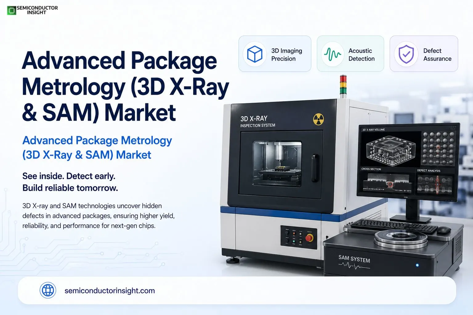
Advanced Package Metrology Market Growth Emerging From Next Generation AI Accelerators
Advanced semiconductor packaging is becoming more complex as chipmakers move toward chiplet integration, stacked die architectures, and ultra-fine interconnect designs. This transition is rapidly increasing the importance of advanced package metrology systems such as 3D X-ray inspection and Scanning Acoustic Microscopy (SAM). These technologies help semiconductor manufacturers detect hidden defects, voids, delamination, solder fatigue, and structural irregularities without physically damaging the package.
The rise of AI accelerators, high bandwidth memory modules, and advanced logic chips is pushing inspection standards beyond conventional optical systems. Semiconductor packaging facilities now require sub-micron inspection precision to maintain yield and long-term device reliability.
According to data published by SEMI, global semiconductor manufacturing equipment spending exceeded USD 100 billion in 2024, with advanced packaging inspection systems representing one of the fastest expanding equipment categories due to increasing packaging complexity.
AI Server Processors Push Non Destructive Inspection into High Demand
The growth of generative AI infrastructure is dramatically increasing demand for advanced package metrology tools. AI server processors contain multiple stacked dies, high-density interconnects, and advanced thermal management structures that are difficult to inspect using traditional methods.
- Modern AI GPUs and accelerators often integrate thousands of microbumps connecting logic and memory stacks.
- Even microscopic voids or bonding inconsistencies can reduce performance or create thermal instability during large-scale AI workloads.
Several semiconductor packaging companies in Taiwan, South Korea, and the United States are expanding 3D X-ray inspection capacity to support advanced AI chip production. Industry publications from engineering organizations have highlighted increasing adoption of computed tomography X-ray systems capable of producing high-resolution volumetric scans for advanced package analysis.
To Stay Tuned with More meaningful and In-Depth Insights, Do Visit here: https://semiconductorinsight.com/report/advanced-package-metrology-3d-x-ray-sam-market/
Scanning Acoustic Microscopy Moves beyond Failure Analysis Labs
- Scanning Acoustic Microscopy, commonly called SAM, was traditionally associated with failure analysis laboratories. Today, it is becoming a frontline process control tool inside high-volume packaging facilities.
- SAM systems use high-frequency ultrasound waves to identify internal defects such as cracks, voids, package delamination, and moisture intrusion. Since advanced semiconductor packages contain multiple bonded layers, even small interface separations can compromise electrical and thermal reliability.
- Automotive semiconductor manufacturers are increasingly integrating SAM systems into reliability testing workflows for power electronics and ADAS Electric vehicle control systems operate under high thermal stress conditions, making defect-free packaging essential for long operational lifecycles.
- In 2025, several automotive chip suppliers expanded acoustic imaging deployment for silicon carbide power module inspection as EV adoption continued rising globally.
Chiplet Architectures Reshape Inspection Requirements
The semiconductor industry is moving away from monolithic chip scaling toward chiplet-based architectures. This transition significantly increases the importance of package-level metrology.
Chiplets allow manufacturers to combine multiple functional dies within a single package, improving performance while reducing manufacturing complexity at advanced process nodes. However, these architectures create intricate bonding layers and interconnect pathways that require advanced imaging systems for inspection.
Major semiconductor manufacturers have introduced multi-die processors integrating CPUs, GPUs, AI engines, and memory stacks inside single advanced packages. This complexity has elevated the role of 3D X-ray systems capable of reconstructing internal package geometries in real time.
The Institute of Electrical and Electronics Engineers has published multiple technical studies emphasizing the importance of advanced inspection technologies for ensuring long-term reliability in heterogeneous integration platforms.
Factory Automation Is Entering the Inspection Layer
- Semiconductor factories are increasingly integrating AI-enabled metrology platforms into automated production environments. Modern inspection systems can now classify defects automatically, reducing operator dependency and accelerating production throughput.
- Machine learning algorithms are being trained to identify solder void patterns, package warpage, and bonding irregularities across thousands of semiconductor packages per hour. This shift is helping manufacturers reduce false positives while improving defect traceability across packaging lines.
- Leading semiconductor manufacturing facilities are connecting X-ray inspection systems directly with factory execution software to enable predictive maintenance and real-time quality analytics. This smart factory integration is becoming especially important as advanced packaging facilities scale production for AI and data centre chips.
Thermal Management Becomes a Packaging Inspection Priority
As processors become more powerful, thermal management inside semiconductor packages is becoming increasingly critical. Advanced package metrology systems are now being used to evaluate thermal interface materials, underfill consistency, and heat dissipation structures.
High-performance AI processors can consume more than 700 watts of power within densely packed systems. Any inconsistency in thermal pathways may create localized overheating that reduces device lifespan or causes operational instability.
3D X-ray inspection technologies are increasingly being used to verify thermal bonding quality in advanced cooling structures, including vapor chambers and liquid-assisted package assemblies. This trend is particularly visible in high-performance computing infrastructure and hyperscale data centre deployments.
Quantum Computing Packaging Expands Precision Inspection Needs
- Emerging quantum computing hardware is creating another specialized application area for advanced package metrology. Quantum processors require ultra-sensitive packaging structures capable of maintaining signal integrity at extremely low temperatures.
- Research laboratories and semiconductor development centres are using advanced X-ray and acoustic inspection systems to evaluate superconducting interconnects and cryogenic package reliability. Even microscopic structural inconsistencies can interfere with quantum coherence performance.
As quantum hardware development accelerates globally, advanced package metrology technologies are expected to play a growing role in ensuring precision assembly and defect-free packaging performance for next-generation computing platforms.

Comments (0)