
Advanced Chip Architectures Rising with Solder Ball for Advanced Packaging Market
Solder Ball for Advanced Packaging Market refers to the industry focused on the production, supply, and application of microscopic solder spheres used to create electrical connections in next-generation semiconductor packaging technologies.
In the world of semiconductors, some of the most critical innovations are almost invisible to the naked eye. Solder balls microscopic spheres of metal have become essential in enabling today’s high-performance chips. These tiny interconnects sit beneath integrated circuits, forming both electrical and mechanical connections between chips and substrates or printed circuit boards.
Where They Are Used?
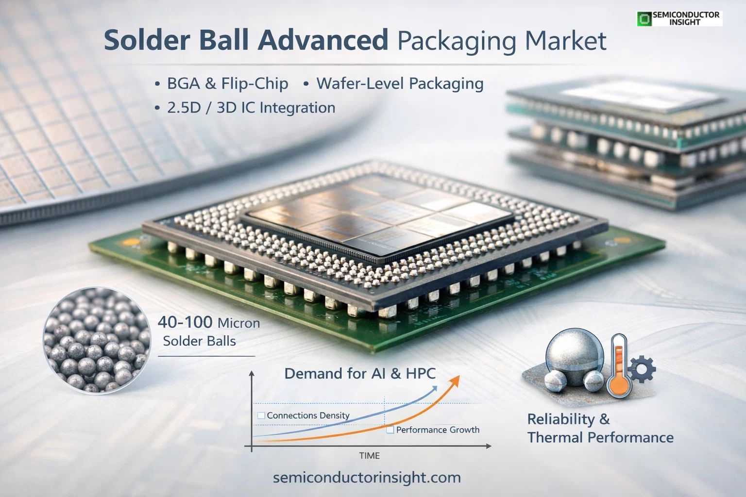
- Ball Grid Array (BGA) – where solder balls form the external connection points under a chip package
- Flip-Chip Packaging – where the chip is flipped and connected directly to a substrate using solder bumps
- Wafer-Level Packaging (WLP) – enabling compact, high-performance chip designs
- 2.5D and 3D IC Packaging – used in high-end processors and memory stacks
Where Packaging Meets Performance Engineering
Advanced packaging is no longer just a backend process it is a performance enabler. Solder balls play a key role in connecting dies within complex structures such as flip-chip ball grid arrays and wafer-level chip scale packages.
The demand for higher input-output density means more connections in smaller areas. Today’s packages can contain thousands of solder balls arranged in dense grids, allowing chips to communicate faster while reducing signal loss. This is particularly important for applications like AI accelerators and high-performance computing systems, where data transfer speed directly impacts efficiency.
Access the Latest Insights from Our Newly Released Study: https://semiconductorinsight.com/report/solder-ball-advanced-packaging-market/
Shrinking Dimensions and Precision Challenges
One of the most striking trends is the rapid reduction in solder ball size. In advanced packaging, diameters have dropped below 100 micrometres, with some designs approaching 40-50 micrometres.
At this scale, even minor inconsistencies can lead to performance issues. Variations in size, oxidation during processing, or improper alignment can cause defects such as bridging or voids. These challenges require highly controlled manufacturing environments and precision engineering techniques, increasing both complexity and cost.
Yet, this miniaturization is essential. Smaller solder balls enable tighter pitches, which in turn allow more compact and powerful semiconductor devices a necessity in smartphones, wearables, and next-generation computing hardware.
Demand Explosion Driven by AI and Data Infrastructure
- The surge in artificial intelligence workloads and cloud computing has significantly amplified the need for advanced packaging solutions. Data centers, GPUs, and AI chips require high-density interconnects that only solder ball-based packaging can reliably deliver.
- In practical terms, a single high-end processor package may contain thousands of solder connections, each contributing to power delivery, signal routing, and thermal stability. This scale highlights how even the smallest components are critical to enabling large-scale digital infrastructure.
Material Innovation Changing the Game
Traditional solder balls are primarily made from tin-based alloys, often combined with silver and copper to enhance reliability. However, evolving performance requirements are driving new material innovations.
Engineers are experimenting with copper-core solder balls to improve heat dissipation, as well as alloy modifications that reduce electro migration a common failure mechanism in high-density interconnects. Enhanced thermal conductivity is becoming increasingly important as chips generate more heat due to higher power densities.
At the same time, environmental regulations have pushed the industry toward lead-free compositions, making material science a critical area of differentiation among suppliers.
Reliability under Extreme Conditions
As semiconductor applications expand into automotive, aerospace, and industrial sectors, reliability has become a defining factor. Solder balls must withstand repeated thermal cycles, mechanical stress, and long operational lifetimes.
Failures at the interconnect level can compromise entire systems, making quality control and testing essential. Advanced inspection techniques, including X-ray imaging and automated optical systems, are now standard in ensuring defect-free solder joints.
The challenge intensifies in multi-die packages, where differences in material expansion can create stress points. Managing these factors is crucial for maintaining performance over time, especially in mission-critical applications.
The Backbone of Next Generation Chip Architectures
Solder balls may appear simple, but they are deeply embedded in the evolution of semiconductor technology. As the industry transitions toward heterogeneous integration and chiplet-based designs, their role will only grow more significant.
From enabling ultra-fast data transfer to supporting compact device architectures, solder balls are quietly shaping the future of electronics. In a landscape where innovation often happens at the nanoscale, these microscopic connectors are proving to be one of the most powerful enablers of progress.

Comments (0)