
Solder Ball for Advanced Packaging Market Insights
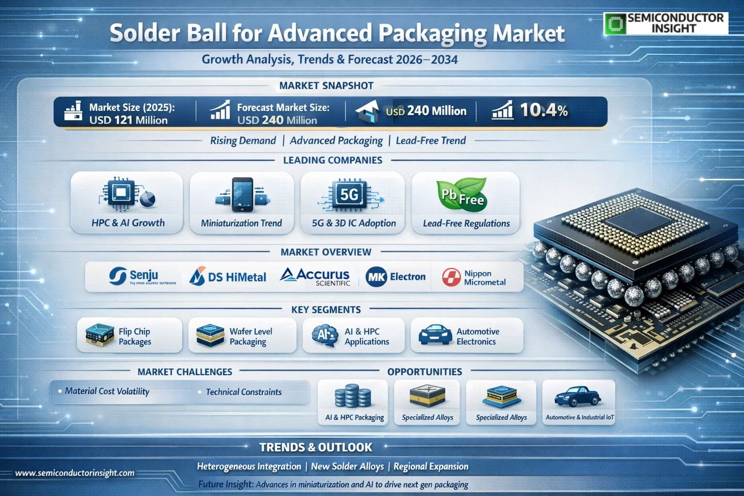
Global solder ball for advanced packaging market size was valued at USD 121 million in 2025. The market is projected to grow from USD 133.6 million in 2026 to USD 240 million by 2034, exhibiting a CAGR of 10.4% during the forecast period.
Solder balls are tin alloy spheres with tin as the main component and other elements such as silver, copper, and nickel as auxiliary components. They play a key role in advanced semiconductor packaging technologies, forming the electrical and mechanical interconnections between a chip and its substrate or between different package components. These critical materials are essential for enabling high-density interconnects in applications like Flip-Chip Ball Grid Array (FCBGA) and Wafer-Level Chip Scale Packaging (WLCSP), which are fundamental to modern electronics miniaturization and performance.
The market is experiencing robust growth driven by several factors, including the relentless demand for smaller, more powerful electronic devices and the subsequent industry shift towards advanced packaging solutions like 2.5D/3D IC integration. Furthermore, the proliferation of artificial intelligence (AI), high-performance computing (HPC), and 5G infrastructure necessitates packaging that can handle higher I/O counts and thermal loads, directly increasing solder ball consumption. While environmental regulations continue to favor lead-free variants, creating a dominant segment, manufacturers face challenges such as material cost volatility and the technical difficulty of producing ever-smaller diameter balls with consistent reliability. Key global players operating in this consolidated market include Senju Metal Industry Co., Ltd., DS HiMetal Co., Ltd., Accurus Scientific Co., Ltd., Nippon Micrometal Corporation, MK Electron Co., Ltd., PhiChem Corporation, Shenmao Technology Inc., Shanghai Tinking Electronic Material Co., Ltd., and Fonton Industrial Corp.
MARKET DRIVERS
Demand from High-Performance Computing and AI Integration
The relentless growth in high-performance computing, artificial intelligence, and 5G infrastructure is a primary catalyst for the Solder Ball for Advanced Packaging Market. These technologies require advanced semiconductor packages with higher I/O density and superior electrical performance, directly increasing the demand for precision-engineered solder balls. The transition to sub-50-micron diameter balls enables the fine-pitch interconnects necessary for 2.5D and 3D integrated circuits, supporting the performance scaling beyond traditional Moore’s Law limitations.
Miniaturization and Heterogeneous Integration
The industry-wide push for miniaturization, particularly in mobile devices and IoT sensors, compels the adoption of advanced packaging solutions like Fan-Out Wafer-Level Packaging (FOWLP) and Chiplet architectures. These methodologies rely heavily on solder ball arrays for die-to-die and die-to-substrate connections. Consequently, the Solder Ball for Advanced Packaging Market is experiencing sustained demand for materials that offer excellent wetting characteristics and low electromigration to ensure reliability in densely packed, multi-die systems.
➤ Global trend towards electric vehicles and advanced driver-assistance systems (ADAS) is creating a robust, high-reliability segment within the market, demanding solder balls with enhanced thermal cycle performance and resistance to harsh automotive environments.
Furthermore, material innovations such as tin-silver-copper (SAC) alloys with reduced silver content or the development of copper-core solder balls are providing solutions for thermal management and mechanical stress, addressing critical challenges in next-generation packages and driving material-specific growth in the sector.
MARKET CHALLENGES
Technical Hurdles in Ultra-Fine-Pitch Applications
A significant challenge for the Solder Ball for Advanced Packaging Market is maintaining consistent quality and reliability at diminishing sizes. As ball diameters shrink below 30 microns, issues like oxidation, bridging during reflow, and void formation become more pronounced and difficult to control. This requires substantial investment in advanced manufacturing equipment, precise atmospheric control during placement, and sophisticated inspection technologies, elevating production costs and complexity for suppliers and packaging houses alike.
Other Challenges
Supply Chain and Raw Material Volatility
The market is sensitive to fluctuations in the prices and availability of key raw metals, particularly tin, silver, and copper. Geopolitical tensions and trade policies can disrupt supply chains, impacting cost stability for solder ball manufacturers. This volatility presents a continuous challenge in offering competitive, long-term pricing to packaging foundries.
Compatibility with Diverse Substrate Materials
The proliferation of new substrate materials, including organic, glass, and silicon, requires solder ball formulations to adapt for optimal adhesion and intermetallic compound formation. Ensuring compatibility across this expanding material landscape without compromising joint strength or reliability is an ongoing technical and R&D challenge for the Solder Ball for Advanced Packaging Market.
MARKET RESTRAINTS
High Capital and R&D Investment Barriers
The capital-intensive nature of the market acts as a major restraint. Establishing production lines capable of manufacturing and handling micron-scale solder balls with extreme purity and sphericity requires significant upfront investment. Furthermore, continuous R&D is essential to develop new alloys and processes for emerging packaging formats. This creates a high barrier to entry for new players and consolidates the market among a few established, technologically adept suppliers, potentially limiting innovation pace and price competition.
Competition from Alternative Interconnect Technologies
Growth of the Solder Ball for Advanced Packaging Market is partially restrained by the development of competing interconnect solutions. Technologies such as copper hybrid bonding, which eliminates solder bumps for direct copper-to-copper fusion, offer potential advantages in density and performance for specific applications. While not a wholesale replacement, the emergence of these alternatives pressures solder ball technology to continually advance to justify its role in the interconnect hierarchy, particularly for the most demanding applications.
MARKET OPPORTUNITIES
Expansion into Advanced Packaging for AI/ML and HPC
The explosive demand for specialized AI/ML accelerators and HPC processors represents a substantial opportunity. These chips utilize the most advanced 2.5D and 3D packaging techniques, which are intensive users of high-performance solder balls. Suppliers who can provide ultra-reliable, low-voiding, and fine-pitch solder ball solutions tailored for these high-value applications can capture significant market share and forge strategic partnerships with leading logic and memory manufacturers.
Development of Specialized Alloys for Emerging Applications
There is a growing opportunity in formulating specialized solder ball alloys. This includes developing low-temperature solder balls for heat-sensitive packages, high-melting-point alloys for hierarchical bonding processes, and compositions with enhanced drop-shock performance for mobile and wearable electronics. Innovation in material science to solve specific thermal, mechanical, or electrical problems in advanced packaging creates differentiated, high-margin product lines within the Solder Ball for Advanced Packaging Market.
Adoption in Mature Markets: Automotive and Industrial IoT
Beyond cutting-edge logic, the automotive electrification and Industrial IoT sectors offer stable, high-growth opportunities. These markets prioritize long-term reliability over ultimate miniaturization, requiring solder balls with proven performance under thermal cycling and harsh conditions. Qualifying products for automotive-grade AEC-Q standards opens a lucrative and durable segment for suppliers in the Solder Ball for Advanced Packaging Market, reducing dependency on the cyclical consumer electronics industry.
Solder Ball for Advanced Packaging Market Trends
Accelerated Demand from Heterogeneous Integration and Miniaturization
The prevailing trend in the Solder Ball for Advanced Packaging market is driven by the electronics industry’s push towards heterogeneous integration and device miniaturization. Advanced packaging technologies like Flip Chip Ball Grid Array (FCBGA) and Wafer-Level Chip Scale Packaging (WLCSP), which are critical for high-performance computing, artificial intelligence, and 5G modules, rely extensively on precision solder balls for electrical interconnection and thermal management. This demand necessitates consistent innovation in alloy composition and ball size uniformity to meet the fine-pitch requirements and reliability standards of next-generation semiconductor devices.
Other Trends
Material Innovation for Enhanced Reliability
A significant industry focus is on developing advanced lead-free solder alloys beyond standard SAC (Tin-Silver-Copper) formulations. Manufacturers are experimenting with additive elements like nickel, bismuth, and germanium to improve electromigration resistance, thermal cycling performance, and drop-shock reliability. This material innovation within the Solder Ball for Advanced Packaging market is essential to support the longevity and durability of packages operating in harsh environments, such as automotive electronics and high-power servers.
Supply Chain Resilience and Geographic Diversification
Recent global supply chain disruptions have prompted a strategic trend towards geographic diversification of solder ball manufacturing and sourcing. While leading players are concentrated in Asia-Pacific, there is a growing emphasis on establishing and qualifying additional production capacity in North America and Europe. This movement aims to create a more resilient supply chain for Global Solder Ball for Advanced Packaging market, mitigating risks and aligning with regional semiconductor fabrication expansion plans to ensure stable supply for critical packaging applications.
COMPETITIVE LANDSCAPE
Key Industry Players
A Specialty Materials Segment Characterized by High Technical Requirements and Regional Concentration
Global solder ball for advanced packaging market exhibits a consolidated structure dominated by a handful of established, technologically adept manufacturers. As of 2025, the top five players collectively commanded a significant revenue share, underscoring the competitive intensity and the high barriers to entry given the stringent quality and precision requirements for flip-chip ball grid array (FCBGA), wafer-level chip-scale packaging (WLCSP), and other advanced applications. Senju Metal from Japan is widely recognized as a global leader, leveraging decades of materials science expertise. Other major manufacturers like DS HiMetal and MK Electron, particularly strong in the South Korean market which services leading semiconductor giants, also hold considerable market influence. Competition is primarily based on alloy composition consistency (lead-free vs. lead-based), ball diameter precision, reliability under thermal stress, and the ability to innovate in tandem with evolving packaging architectures.
Beyond the top-tier players, the landscape includes several prominent niche and regional specialists that contribute to crucial supply chain diversification. Companies such as Accurus Scientific (US) and Nippon Micrometal (Japan) focus on high-purity and specialty alloys catering to specific performance metrics. The Asia-Pacific region, especially China and Taiwan, hosts significant production capabilities with players like Shenmao Technology, Shanghai Tinking, and PhiChem serving both domestic and international demand. Meanwhile, firms like Fonton Industrial represent key manufacturing hubs in Southeast Asia. The competitive dynamics are further influenced by strategic partnerships with semiconductor packaging and test houses, continuous R&D to support miniaturization trends, and compliance with evolving global environmental regulations regarding material composition.
List of Key Solder Ball for Advanced Packaging Companies Profiled
- Senju Metal Industry Co., Ltd.
- DS HiMetal Co., Ltd.
- Accurus Scientific Co., Ltd.
- MK Electron Co., Ltd.
- Nippon Micrometal Corporation
- PhiChem Corporation
- Shenmao Technology Inc.
- Shanghai Tinking Electronic Materials Co., Ltd.
- Fonton Industrial Co., Ltd.
- Indium Corporation
- Alfa Aesar (Thermo Fisher Scientific)
- Duksan Hi-Metal Co., Ltd.
- Yun Zhong Metal Technology Co., Ltd.
- FCT Solder
- Qualitek International, Inc.
Segment Analysis:
| Segment Category | Sub-Segments | Key Insights |
| By Type |
|
Lead-free Solder Balls represent the dominant and technologically progressive segment driven by stringent global environmental regulations like RoHS, which restrict hazardous substances and are critical for electronics exports. This segment’s growth is primarily fueled by its superior performance in high-reliability applications, offering excellent thermal fatigue resistance and mechanical strength required for modern, densely packed semiconductor devices. The transition to lead-free alloys, often SAC-based, is a standard across the electronics supply chain, making this segment non-negotiable for new product designs and a key focus area for material innovation among major manufacturers. |
| By Application |
|
FCBGA (Flip Chip Ball Grid Array) is the leading application segment due to its critical role in high-performance computing, servers, and advanced graphics processing units where thermal management and electrical performance are paramount. This segment demands solder balls with very high consistency in diameter and superior co-planarity to ensure reliable connections for chips with extremely high pin counts. The ongoing drive towards heterogeneous integration and 2.5D/3D packaging architectures further solidifies FCBGA’s position, as these advanced interconnects rely on sophisticated solder ball technologies to function, creating a sustained pipeline for premium, high-margin product demand. |
| By End User |
|
Foundries & OSATs constitute the most influential end-user segment, acting as the primary volume buyers and technology drivers. Their leadership stems from their central position in Global semiconductor manufacturing ecosystem, packaging chips for a vast array of fabless design houses and system companies. This segment exerts significant pressure on solder ball suppliers for continuous innovation in alloy composition and micro-ball sizing to meet evolving packaging roadmaps. Their large-scale, high-mix production environments also prioritize supply chain resilience and stringent quality certification, creating high barriers to entry but rewarding suppliers with deep technical partnerships and long-term contracts. |
| By Alloy Composition |
|
SAC (Tin-Silver-Copper) Alloys are unequivocally the leading material composition, serving as the industry-standard workhorse for most advanced packaging applications. Their dominance is attributed to a well-understood balance of good solderability, respectable mechanical strength, and reliable thermal cycling performance, which has been optimized over decades of research and deployment. While other alloys cater to niche cost or low-temperature requirements, SAC formulations, particularly those with minor doping elements like nickel or bismuth, are at the forefront of development for next-generation packages that must withstand higher power densities and more severe thermal stresses, ensuring their continued central role. |
| By Ball Diameter |
|
Micro Balls (< 100 µm) represent the high-growth, technologically intensive frontier of the market. The relentless drive for miniaturization and higher I/O density in packages like WLCSP and fine-pitch FCBGA is propelling demand for these exceptionally small and precise spheres. This segment commands a significant technical premium due to the extreme manufacturing challenges in achieving perfect sphericity, minimal size variation, and oxidation control at such micro scales. Supplying these balls requires advanced metallurgical processes and cleanroom production, creating a competitive moat for established players and aligning directly with the industry’s roadmap for more compact and powerful electronic devices. |
Regional Analysis: Global Solder Ball for Advanced Packaging Market
Asia-Pacific
The region’s unparalleled electronics manufacturing base, from major foundries to countless component suppliers, creates a seamless, high-volume demand pipeline for solder balls. Proximity between material producers, packaging houses, and end-device manufacturers minimizes logistical friction and fosters collaborative development for customized alloy formulations and sizes.
Asia-Pacific is at the forefront of pioneering advanced packaging architectures such as fan-out wafer-level packaging and 3D IC stacking. This relentless drive for miniaturization and performance pushes solder ball suppliers to innovate in ultra-fine pitch, low-temperature, and high-reliability alloys to meet the exacting standards of leading chip designers.
National strategies, including China’s push for semiconductor independence and South Korea’s focus on memory and foundry leadership, involve substantial public and private funding. These initiatives directly fuel capital expenditures in advanced packaging facilities, creating a stable, long-term demand driver for critical interconnect materials like solder balls.
Demand is buoyed by a broad spectrum of high-growth sectors. The region is a global center for smartphone production, automotive electronics manufacturing, and cloud infrastructure build-out, each requiring advanced packages with specific solder ball performance characteristics, from thermal cycling endurance to electromigration resistance.
North America
North America remains a critical region, characterized by its strength in semiconductor design, R&D, and high-value manufacturing. The demand for solder balls for advanced packaging is heavily influenced by leading fabless companies and IDMs (Integrated Device Manufacturers) based in the United States, which set the performance roadmap for cutting-edge chips. This region drives specifications for advanced packages used in data centers, aerospace, and defense applications, where reliability under extreme conditions is paramount. Collaboration between material science firms, national labs, and semiconductor companies fosters innovation in novel solder alloys, such as those with improved thermal properties for high-power devices. While large-scale volume manufacturing may be concentrated overseas, North America’s role in defining technical requirements and pioneering next-generation packaging concepts ensures it exerts significant influence over Global solder ball market’s evolution.
Europe
Europe holds a notable position in the solder ball for advanced packaging market, distinguished by its focus on specialized, high-reliability applications and automotive-grade electronics. The region’s robust automotive industry, particularly the shift towards electric and autonomous vehicles, demands advanced packaging solutions with exceptional durability and performance under harsh conditions, creating steady demand for specialized solder balls. European semiconductor firms and research institutions are also leaders in power electronics and sensors, areas where packaging integrity is critical. There is a concerted effort to enhance regional semiconductor sovereignty, exemplified by the European Chips Act, which aims to bolster manufacturing capacity. This strategic focus is expected to gradually increase local demand for advanced packaging materials, including high-quality solder balls, while maintaining the region’s reputation for precision engineering and stringent quality standards.
South America
The South American solder ball for advanced packaging market is in a developing phase, with demand primarily linked to the assembly and consumer electronics sectors rather than front-end semiconductor fabrication. Brazil and Mexico are key centers for electronics manufacturing services, supplying regional and sometimes global markets with finished consumer goods. Demand for solder balls is therefore derivative, tied to the assembly of imported semiconductor packages into final products. The market growth is connected to broader economic development, industrial expansion, and increasing technology adoption. While not a primary hub for advanced packaging innovation, the region presents a growing consumption base. Its market dynamics are influenced by trade policies, foreign investment in manufacturing, and the gradual sophistication of local electronics production, which may slowly increase the need for more advanced interconnect solutions.
Middle East & Africa
The Middle East & Africa region represents an emerging and strategically diversifying market. While current direct consumption of solder balls for advanced packaging is relatively modest, significant investments in technology infrastructure, particularly in Gulf Cooperation Council (GCC) nations, are laying the groundwork for future growth. These economies are actively investing in data centers, telecommunications for 5G rollout, and smart city initiatives, all of which rely on advanced semiconductor packages. The region’s focus is largely on the deployment and integration of high-tech systems rather than component manufacturing. However, strategic initiatives to develop knowledge-based economies could foster niche R&D activities in the longer term. For now, the market is characterized by import-dependent demand, with growth closely tied to technology adoption rates and large-scale infrastructure projects that incorporate advanced electronics.
Report Scope
This market research report provides a comprehensive analysis of the Solder Ball for Advanced Packaging Market , covering the forecast period 2026–2034. It offers detailed insights into market dynamics, technological advancements, competitive landscape, and key trends shaping the industry.
Key focus areas of the report include:
- Market Overview: The report begins with an overview outlining the current market scenario, key growth indicators, and industry transformation drivers. It discusses macroeconomic factors, demand–supply balance, regulatory landscape, and the strategic role of advanced packaging components in enabling next-generation electronics across industries such as computing, telecommunications, automotive, and consumer electronics.
- Market Size & Forecast: Historical data and future projections for revenue, unit shipments, and market value across major regions and segments.
- Segmentation Analysis: Detailed breakdown by product type (Lead-free, Lead-based), application (FCBGA, WLCSP, Others), and end-user industry to identify high-growth segments and investment opportunities.
- Regional Insights: Insights into market performance across North America, Europe, Asia-Pacific, Latin America, and the Middle East & Africa, including country-level analysis for key markets like the U.S., China, Japan, and South Korea.
- Competitive Landscape: Profiles of leading market participants, including their product offerings, R&D focus, manufacturing capacity, pricing strategies, and recent developments such as mergers, acquisitions, and partnerships.
- Technology Trends & Innovation: Assessment of emerging packaging technologies, material advancements, integration trends, and evolving industry standards for semiconductor assembly.
- Market Drivers & Restraints: Evaluation of factors driving market growth along with challenges, supply chain constraints, raw material price volatility, regulatory issues, and market-entry barriers.
- Stakeholder Insights: Insights for component suppliers, semiconductor manufacturers, packaging foundries, investors, and policymakers regarding the evolving ecosystem and strategic opportunities.
Primary and secondary research methods are employed, including interviews with industry experts, data from verified sources, and real-time market intelligence to ensure the accuracy and reliability of the insights presented. The report is based on extensive surveys of manufacturers, suppliers, distributors, and industry experts conducted by MARKET MONITOR GLOBAL, INC (MMG).
FREQUENTLY ASKED QUESTIONS:
What is the current market size and growth forecast for the Solder Ball for Advanced Packaging Market?
-> Global Solder Ball for Advanced Packaging Market was valued at USD 121 million in 2025 and is projected to reach USD 240 million by 2034, growing at a CAGR of 10.4% during the forecast period.
Which key companies operate in the Solder Ball for Advanced Packaging Market?
-> Key players include Senju Metal, DS HiMetal, Accurus Scientific, Nippon Micrometal, MK Electron, PhiChem, Shenmao, Shanghai Tinking, and Fonton Industrial, among others. Global top five players held a significant revenue share in the market in 2025.
What are the key applications of solder balls in advanced packaging?
-> Solder balls play a key role in advanced packaging technologies such as Flip Chip Ball Grid Array (FCBGA) and Wafer-Level Chip Scale Packaging (WLCSP), serving as critical interconnects for high-performance semiconductors.
What are the main segments in this market?
-> The market is segmented by type into Lead-free Solder Balls and Lead Solder Balls, and by application into FCBGA, WLCSP, and Others. The Lead-free Solder Balls segment is a significant and growing category.
What is the regional outlook for the Solder Ball for Advanced Packaging Market?
-> This is a global market with key geographical segments including North America, Europe, Asia, South America, and the Middle East & Africa. The U.S. and China are major country-level markets within this landscape.

Get Sample Report PDF for Exclusive Insights
Report Sample Includes
- Table of Contents
- List of Tables & Figures
- Charts, Research Methodology, and more...




