
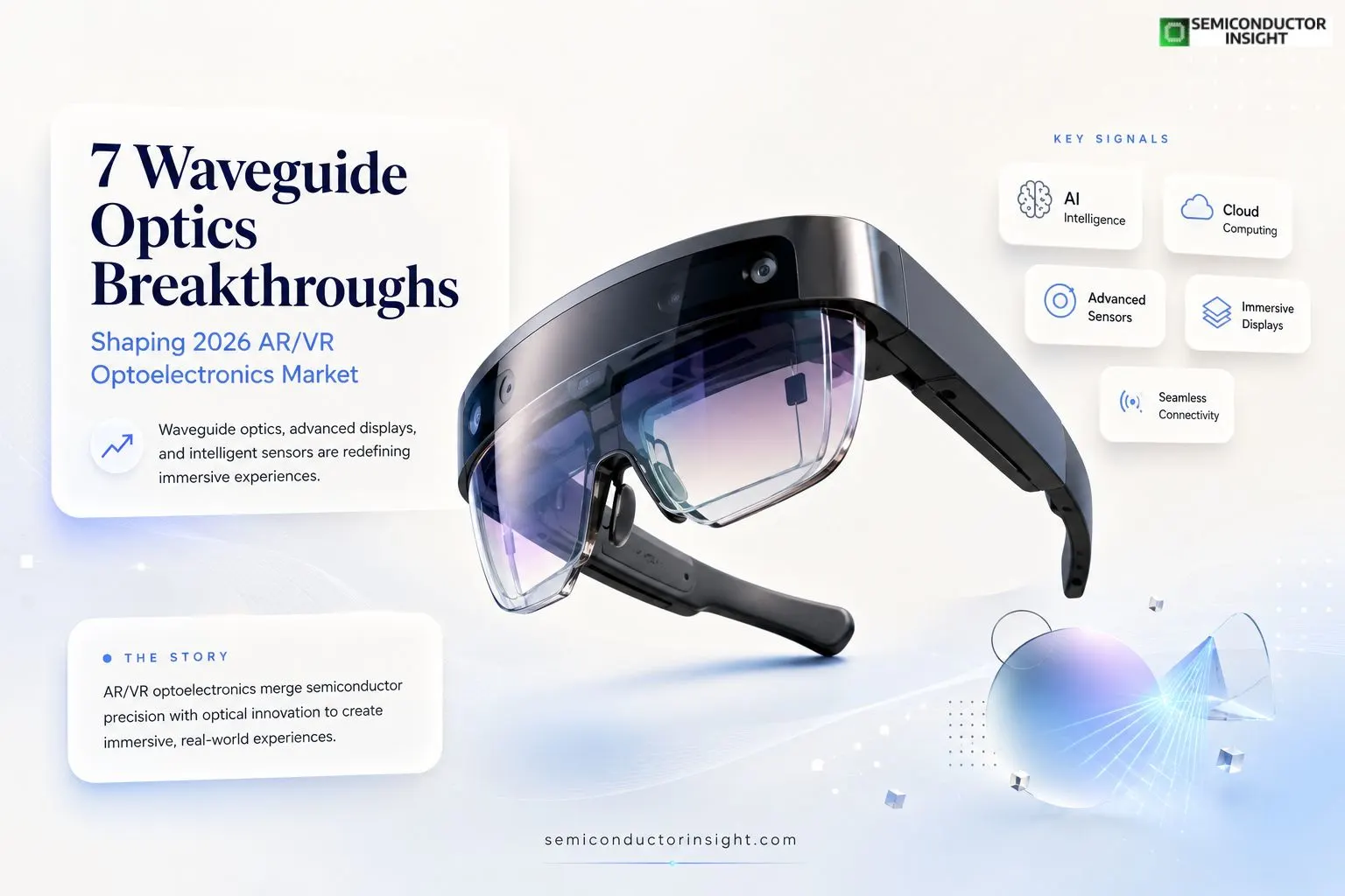
7 Waveguide Optics Breakthroughs Shaping 2026 AR/VR Optoelectronics Market
The AR/VR optoelectronics domain sits at the intersection of semiconductor miniaturization and immersive visual technologies. These systems rely on compact displays, advanced waveguides, and precision sensors to deliver seamless overlays or fully virtual environments.
Current entries on augmented and virtual reality outline how near-eye displays use microdisplays like OLED-on-silicon or emerging MicroLED arrays to project high-resolution imagery directly in front of the user’s eyes.
Waveguide Structures Enabling See-Through Experiences
Optical combiners form the backbone of many AR devices, directing light from microdisplays into the user’s field of view while allowing real-world visibility. Surface relief gratings etched into glass or plastic substrates guide light through total internal reflection.
Microsoft’s HoloLens series employs diffractive waveguide technology, stacking multiple layers for full-color output across a reasonable field of view. Similar approaches appear in Magic Leap devices, which utilize liquid crystal on silicon panels paired with proprietary light field techniques to reduce bulk.
Light Path in Typical Waveguide AR System
Microdisplay Projection → Input Coupler Grating → Propagation via Total Internal Reflection → Output Expander Grating → Retina Projection. This sequence maintains image integrity while minimizing device weight
Microdisplay Evolution and Brightness Challenges
Ø MicroOLED and MicroLED panels deliver the pixel densities necessary for comfortable long-term wear. Apple Vision Pro showcases high pixel-per-inch counts through custom silicon-based displays, supporting detailed mixed reality overlays.
Ø Research documented in scientific articles highlights MicroLED potential for peak brightness levels exceeding thousands of nits, crucial for outdoor AR use where ambient light competes with virtual content.
Comparative Display Characteristics in Current Devices
The following examples highlight how major XR devices differ in display technology, resolution, and key optoelectronic features. Apple Vision Pro uses MicroOLED displays with an approximate resolution of 3660 x 3200 per eye and includes eye-tracking integration, while the Meta Quest Series typically uses fast LCD or OLED panels with resolution that varies by model and relies on pancake lens optics.
HoloLens 2 is built on LCoS display technology, offers an approximate resolution of 2048 x 1080, and uses diffractive waveguides for its mixed reality experience. This comparison is based on public technical overviews and hardware specifications from Wikipedia.
Sensor Integration for Spatial Awareness
ü Optoelectronic sensors including depth cameras, IMUs, and infrared illuminators enable precise head and hand tracking.
ü Time-of-flight or structured light modules feed data to on-board processors, creating accurate environmental maps.
ü Meta’s Reality Labs platforms incorporate multiple sensor arrays to support pass-through video and gesture recognition, blending physical and digital spaces effectively.
Take a Quick Glance at Our In-Depth Analysis Report: https://semiconductorinsight.com/report/ar-vr-optoelectronics-market/
Real-World Deployments across Industries
Enterprise applications demonstrate practical impact. Manufacturing facilities use AR headsets for overlaying assembly instructions, reducing errors through real-time visual guidance. Medical training programs leverage VR optoelectronics for immersive simulations, with systems providing stereoscopic views and haptic feedback integration.
In consumer spaces, standalone headsets support gaming and virtual meetings, with shipments of VR/MR devices reaching around 9.6 million units globally in 2024 according to aggregated industry shipment trackers.
Ongoing examples include pilots in architecture where professionals walk through holographic building models, and education platforms delivering interactive lessons via lightweight AR glasses.
Ø Metasurface and Holographic Techniques
Emerging optics employ nanoscale structures to manipulate light more efficiently than traditional lenses. These flat optics reduce thickness and weight, addressing common comfort complaints. Publications from optics research describe how metasurfaces enable wider fields of view without distortion, pushing boundaries for everyday wearable use.
Ø Power and Thermal Management in Compact Form Factors
Optoelectronic components generate heat in confined spaces, requiring innovative cooling and efficient drivers. VCSEL arrays for eye tracking and illumination optimize power draw, extending battery life in mobile configurations. Government-supported research through bodies like NSF explores materials that improve energy efficiency in these subsystems.
Collaboration Examples in Development
Partnerships between semiconductor foundries and device makers accelerate prototyping. Efforts focus on monolithic integration of displays with processing circuits, reducing latency for more natural interactions. Public case descriptions from technology demonstrations show progress toward lighter designs suitable for all-day wear.
The AR/VR optoelectronics landscape advances through layered optical innovations, semiconductor scaling, and practical integration across use cases. From enterprise tools to consumer entertainment, these technologies refine how digital information merges with physical reality, building on established engineering foundations while exploring novel photonic approaches.
Continued refinements in materials and architectures promise broader accessibility and richer experiences in the years ahead.

Comments (0)