300mm Wafer Fabs vs. Emerging Specialty Fabs in the Semiconductor Equipment Market 2026
The semiconductor industry is often discussed through the lens of chips, processors, and artificial intelligence, yet the machinery used to manufacture those chips has become one of the most strategically important segments of the technology ecosystem. The Semiconductor Equipment Market sits at the center of global digital transformation, supplying the advanced tools required to fabricate processors, memory devices, power semiconductors, and AI accelerators that power everything from smartphones to hyperscale data centers.
– According to industry statistics published by SEMI, global semiconductor manufacturing equipment sales surpassed USD 117 billion in 2024, marking one of the highest spending cycles ever recorded.
– The momentum has continued into 2026 as governments and manufacturers invest heavily in domestic semiconductor production capabilities.
The New Factory Race Is Being Measured in Cleanrooms
A decade ago, semiconductor competition focused primarily on chip design. Today, attention has shifted toward fabrication capacity.
Across the United States, Taiwan, South Korea, Japan, India, Germany, and Singapore, dozens of new fabrication facilities are either under construction or entering production phases. Modern fabs require thousands of specialized equipment systems ranging from lithography tools and deposition systems to etching, metrology, and wafer inspection platforms.
Snapshot of Modern Fab Scale
These facilities are built at an extraordinary scale, with cleanroom areas ranging from 50,000 to more than 100,000 square meters and construction costs often reaching USD 10-30+ billion.
Each fab typically runs on 300 mm wafers, processes 1,000-1,500+ steps per chip, and depends on several thousand equipment systems to maintain production. Together, these figures show why semiconductor fabs are considered some of the most advanced and complex manufacturing environments ever created.
Semiconductor Equipment Market Size through Manufacturing Activity
Instead of measuring the market solely by revenue, many analysts increasingly evaluate semiconductor equipment demand through manufacturing output indicators.
Industry Activity Indicators;
Global Semiconductor Equipment Sales (SEMI)
↓
USD 106 Billion (2023)
↓
USD 117 Billion+ (2024)
↓
Continued Expansion Through AI-Led Fab Investments
At the same time, global installed wafer fabrication capacity has exceeded 30 million wafers annually across leading manufacturing hubs, creating sustained demand for process equipment and production upgrades.
Why AI Servers Are Ordering More Equipment than Smartphones?
One of the most significant changes in 2026 is the growing influence of artificial intelligence infrastructure.
AI accelerators require advanced nodes, high-bandwidth memory (HBM), chiplet architectures, and advanced packaging technologies. Producing these devices demands additional layers of lithography, inspection, deposition, and testing equipment compared with conventional semiconductor products.
Recent examples include:
· Expansion of advanced packaging lines supporting AI processors
· High-bandwidth memory production investments in South Korea
· New logic chip manufacturing facilities announced in the United States and Europe
· AI-focused wafer capacity expansions across Taiwan
As a result, equipment purchases are increasingly tied to data center growth rather than consumer electronics demand alone.
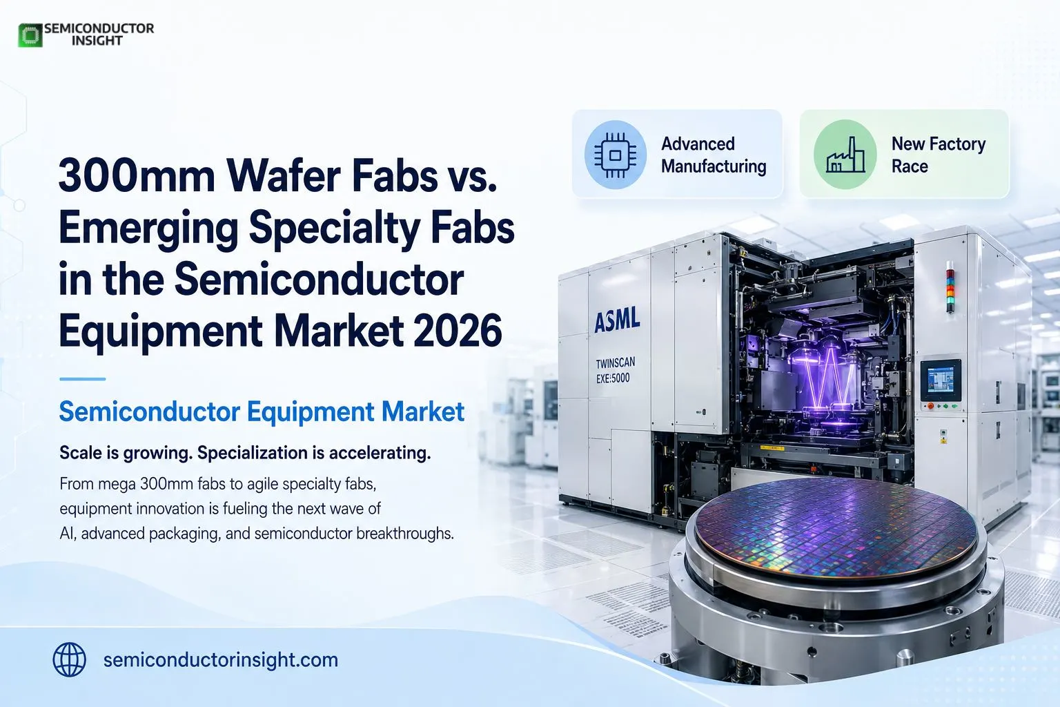
The High-NA EUV Era Begins
One of the most discussed developments in semiconductor manufacturing is High Numerical Aperture Extreme Ultraviolet (High-NA EUV) lithography.
The first commercial High-NA EUV systems entered deployment in advanced manufacturing facilities during 2025 and 2026. These machines are among the most complex industrial tools ever produced.
Technology Progression Map
DUV Lithography
↓
EUV Lithography
↓
High-NA EUV
↓
Sub-2 Nanometer Manufacturing
↓
Advanced AI Processor Production
Each transition requires substantial upgrades throughout the semiconductor equipment ecosystem.
Beyond Wafer Fabrication the Rise of Packaging Equipment
Chip performance improvements are increasingly being achieved through packaging innovations rather than transistor scaling alone.
Advanced packaging technologies such as:
ü Chiplets
ü 2.5D integration
ü 3D stacking
ü Hybrid bonding
ü Fan-out packaging
These are generating demand for entirely new categories of semiconductor manufacturing equipment.
Industry publications from IEEE and leading semiconductor conferences indicate that advanced packaging investments now represent one of the fastest-growing equipment segments supporting AI and high-performance computing applications.
For More Detailed Insights, You Can Surf Our Latest Related Report Here: https://semiconductorinsight.com/report/semiconductor-equipment-for-advanced-packaging-market/
Factory Intelligence Replaces Traditional Monitoring
Modern semiconductor equipment no longer functions as standalone machinery.
Today’s manufacturing systems generate terabytes of operational data every day.
Smart Equipment Workflow
Sensor Networks
↓
Real-Time Process Monitoring
↓
Machine Learning Analytics
↓
Predictive Maintenance
↓
Yield Optimization
↓
Autonomous Process Adjustments
This digital manufacturing approach helps fabs improve yields while minimizing costly downtime.
The Equipment Layer behind Every Technology Breakthrough
Whether enabling AI servers, autonomous vehicles, industrial automation systems, advanced smartphones, or next-generation memory technologies, semiconductor equipment forms the foundation of modern electronics manufacturing.
As global investments continue flowing into fabrication facilities, advanced packaging plants, and AI infrastructure projects, the industry’s most important innovations increasingly begin not with the chip itself, but with the highly specialized equipment that makes those chips possible.
Comments (0)