

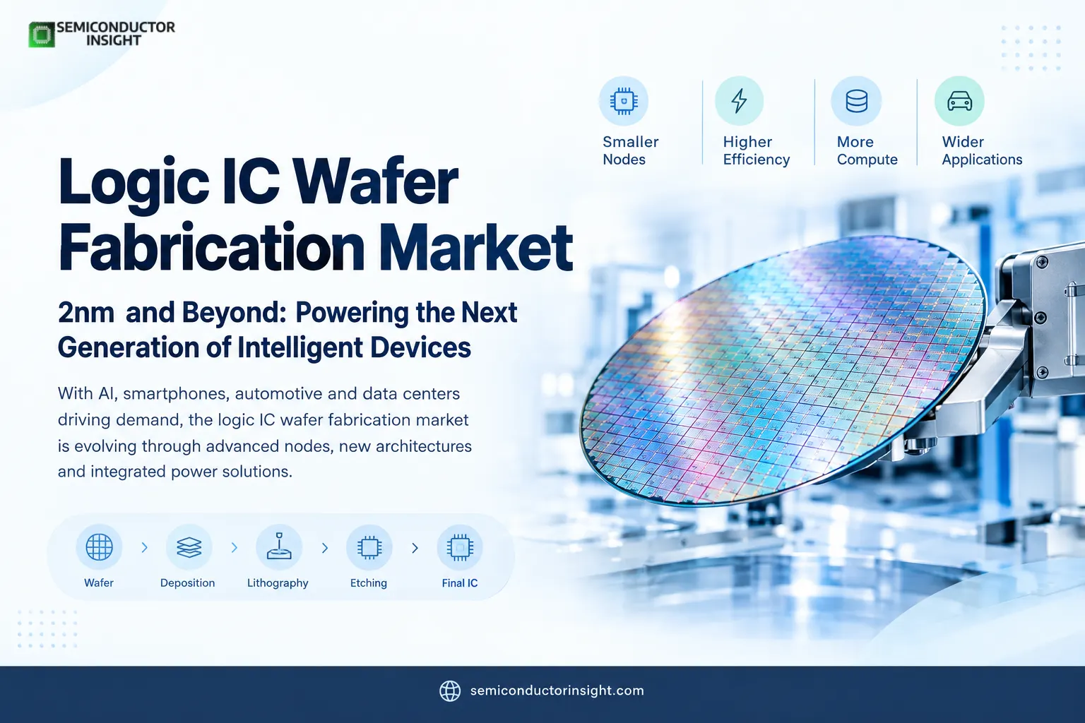
2026 Semiconductor Fab Expansion Puts the Logic IC Wafer Fabrication Market at the Center of AI Infrastructure
The logic semiconductor industry is entering a manufacturing phase where transistor architecture, wafer diameter, power delivery, lithography and process integration are becoming inseparable.
Artificial intelligence is intensifying demand for high-performance processors, while smartphones, automotive electronics, data centers and edge computing continue requiring increasingly efficient logic silicon. This is placing the Logic IC Wafer Fabrication Market at the center of the semiconductor industry’s shift toward 2nm-class production.
The Wafer Is Becoming a Strategic Production Asset
Modern logic fabrication is overwhelmingly built around 300mm silicon wafers because their larger surface area allows more dies to be produced from each wafer than smaller formats. SEMI’s 2026 300mm Fab Outlook tracks 424 fabs and production lines worldwide and projects global 300mm front-end fab equipment spending at $149 billion in 2026. Logic and microelectronics, including foundry production, are expected to remain the largest product category through 2031.
The industry’s scale can be visualized as:
300mm silicon wafer → deposition → lithography → etching → implantation → metallization → inspection → wafer test → dicing → packaged logic IC
Each additional process generation adds more complexity to this sequence.
2nm Has Moved From Roadmap to Production
One of the defining developments of 2026 is that 2nm manufacturing is no longer merely a technology demonstration. TSMC reports that its N2 process entered volume production in the fourth quarter of 2025 and is ramping during 2026. The technology uses a first-generation nanosheet transistor architecture rather than the FinFET structure used in earlier generations.
TSMC’s 2025 annual report states that 3nm represented 24% of its total wafer revenue during 2025, while 2nm entered high-volume manufacturing late in the year. Its N2P and A16 technologies are scheduled for volume production in the second half of 2026.
This creates a rapidly evolving manufacturing ladder:
7nm FinFET → 5nm FinFET → 3nm FinFET → 2nm nanosheet → A16 and subsequent sub-2nm generations
GAA Architecture Changes the Front End of the Process
- Gate-all-around transistor structures are becoming one of the defining process changes in advanced logic fabrication. Instead of controlling the channel from multiple sides as in FinFET architecture, GAA structures surround the channel with the gate, improving electrostatic control as dimensions shrink.
- Intel’s 18A platform combines RibbonFET GAA transistors with PowerVia backside power delivery. Intel says 18A entered production in 2025 and is in high-volume production in the United States, while its enhanced 18A-P technology entered risk production in 2026.
- The manufacturing significance goes beyond transistor dimensions because power delivery itself is being redesigned.
Backside Power Is Rewriting Wafer-Level Integration
Traditional logic chips route power and signals through structures positioned above the transistor layer. Backside power technologies move major power-distribution structures toward the rear of the wafer or die.
Intel’s PowerVia embeds nanoscale through-silicon vias into standard cells and relocates coarse-pitch power metals to the backside. Intel reports that PowerVia can reduce worst-case dynamic voltage droop by as much as 10 times and enable up to 11% block-level area compaction in its internal comparisons.
TSMC is pursuing a similar direction with A16, which integrates nanosheet transistors with a backside power rail designed particularly for demanding high-performance computing designs.
For additional report info, feel free to view our most recent edition: https://semiconductorinsight.com/report/logic-ic-wafer-fabrication-market/
AI Is Increasing the Value of Advanced Logic Capacity
AI accelerators are creating a different type of wafer-fabrication requirement. Higher transistor density must be accompanied by better power efficiency, faster interconnects and increasingly sophisticated packaging.
SEMI projects global 7nm-and-below capacity to rise from approximately 850,000 wafers per month in 2024 to 1.4 million wafers per month by 2028, a roughly 69% increase. The organization attributes the expansion largely to accelerating demand for generative AI and advanced computing.
Meanwhile, worldwide silicon wafer shipments reached 3,313 million square inches in Q3 2025, with 300mm shipments benefiting from advanced logic, cloud infrastructure and memory demand.
Fabrication Is Becoming a Co-Design Exercise
- The modern Logic IC Wafer Fabrication Market is increasingly shaped by design-technology co-optimization rather than transistor scaling alone.
- Samsung Foundry’s 2026 strategy, for example, combines 2nm GAA process development with an expanding AI design ecosystem involving chiplets, 3D ICs, advanced packaging and high-bandwidth interconnects.
- That shift changes the role of the wafer fab. It is no longer simply the location where a circuit is physically manufactured.
- Process architecture, design libraries, power delivery, packaging and manufacturing yield increasingly have to be engineered as one system.
The New Manufacturing Equation
AI workload → advanced chip architecture → 2nm/3nm process → GAA transistor → backside power → advanced packaging → higher compute density
This chain explains why wafer fabrication is becoming one of the most closely watched layers of the semiconductor value chain in 2026. The industry’s next gains will depend not on a single smaller node, but on how effectively fabs combine wafer scale, transistor architecture, lithography, power delivery, process control and packaging into commercially manufacturable logic platforms.

Comments (0)