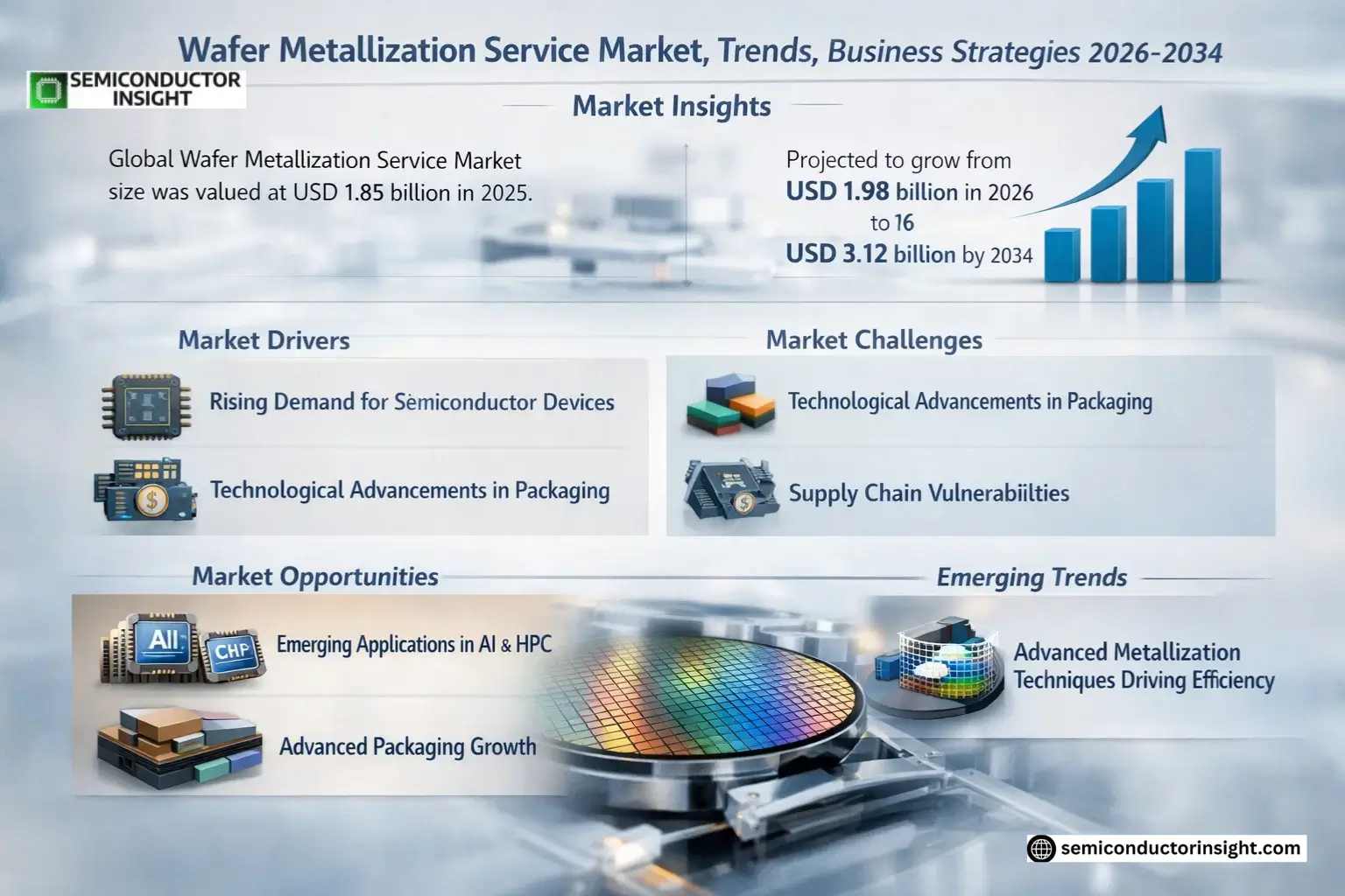
Market Insights
Global Wafer Metallization Service Market size was valued at USD 1.85 billion in 2025. The market is projected to grow from USD 1.98 billion in 2026 to USD 3.12 billion by 2034, exhibiting a CAGR of 6.7% during the forecast period.
Wafer metallization services involve depositing thin metal layers on semiconductor wafers to create electrical interconnects, essential for integrated circuit functionality. These processes include frontside and backside metallization techniques such as sputtering, evaporation, and electroplating, utilizing materials like aluminum, copper, and gold.
The market growth is driven by increasing demand for advanced semiconductor devices in consumer electronics, automotive applications, and communication technologies. Key players such as Power Master Semiconductor Co., Ltd., JX Advanced Metals Corporation, and Vanguard International Semiconductor Corporation are expanding their capabilities to meet rising demand for high-performance metallization solutions.
MARKET DRIVERS
Rising Demand for Semiconductor Devices
Global Wafer Metallization Service Market is experiencing significant growth due to the increasing demand for semiconductor devices across industries such as consumer electronics, automotive, and telecommunications. With the semiconductor industry projected to grow at 7% CAGR through 2030, wafer metallization services are becoming critical for advanced chip packaging and interconnect solutions.
Technological Advancements in Packaging
Emerging technologies like 2.5D/3D IC packaging and wafer-level packaging (WLP) are driving innovation in wafer metallization processes. The need for finer pitch interconnects and improved thermal management is pushing metallization service providers to develop advanced deposition techniques with higher precision.
Additionally, the transition to copper metallization over traditional aluminum processes continues to gain momentum, offering better conductivity and electromigration resistance for high-performance applications.
MARKET CHALLENGES
High Capital Investment Requirements
Establishing wafer metallization service capabilities requires significant capital expenditure for specialized equipment like PVD and CVD systems. The average cost for a complete wafer metallization line can exceed USD 20 million, creating substantial barriers to entry for new market players.
Other Challenges
Yield Optimization Complexities
Maintaining high yields in wafer metallization processes becomes increasingly challenging at advanced nodes below 10nm, where defect density control is critical for cost-effective production.
Material Compatibility Issues
The integration of new metallization materials with existing semiconductor processes requires extensive process development and qualification, slowing time-to-market for new solutions.
MARKET RESTRAINTS
Supply Chain Vulnerabilities
Wafer Metallization Service Market faces constraints from global semiconductor supply chain disruptions, particularly in the availability of high-purity metal targets and specialty gases. Recent geopolitical developments have exacerbated these issues, leading to extended lead times for critical materials.
MARKET OPPORTUNITIES
Emerging Applications in AI and HPC
The rapid growth of AI chips and high-performance computing applications presents significant opportunities for wafer metallization service providers. These applications demand advanced metallization schemes capable of handling higher current densities and improved signal integrity at ultra-fine geometries.
Advanced Packaging Growth
The shift toward heterogeneous integration and chiplet-based designs is creating new requirements for wafer-level redistribution layers (RDLs) and through-silicon vias (TSVs), driving demand for specialized metallization services.
Emerging Wafer Metallization Service Market Trends
Advanced Metallization Techniques Driving Efficiency
Wafer Metallization Service Market is witnessing significant advancements in deposition technologies, particularly for frontside metallization applications. Leading service providers are adopting atomic layer deposition (ALD) and physical vapor deposition (PVD) methods to achieve superior uniformity and conductivity. This technological evolution directly addresses the growing demand for higher-density interconnects in semiconductor devices.
Other Trends
Materials Innovation for Enhanced Performance
Service providers are increasingly utilizing novel metal alloys and barrier materials to improve electromigration resistance. Copper metallization remains dominant, but innovations in aluminum alloys and barrier layers are gaining traction for specific high-reliability applications in automotive and industrial electronics.
Regional Specialization in Service Offerings
The Asia-Pacific region continues to expand its Wafer Metallization Service capabilities, with Taiwan, China, and South Korea emerging as key hubs. North American and European providers are focusing on specialty applications and low-volume, high-mix production scenarios, creating distinct market segments within the global landscape.
Application-Specific Solutions
Metallization services are becoming more tailored to end-use applications, with distinct approaches for consumer electronics (emphasizing cost-efficiency) versus automotive or industrial applications (prioritizing reliability and thermal performance). This specialization is driving diversification among service providers’ portfolio offerings.
Consolidation and Partnerships
The market is seeing increased strategic partnerships between metallization service providers and semiconductor manufacturers to ensure supply chain stability. Recent collaborations have focused on developing customized metallization solutions for advanced packaging applications in 5G and IoT devices.
COMPETITIVE LANDSCAPE
Key Industry Players
Strategic Positioning in the USD Million Wafer Metallization Service Market
Global Wafer Metallization Service Market is moderately consolidated with Power Master Semiconductor Co., Ltd., JX Advanced Metals Corporation, and Vanguard International Semiconductor Corporation collectively holding significant market share. These industry leaders dominate through advanced deposition technologies, regional manufacturing footprints, and strategic partnerships with semiconductor foundries. PacTech and Axetris have emerged as technology specialists, focusing on niche metallization processes for MEMS and power devices.
Regional players like CHIPBOND Technology Corporation and Huahong Group maintain strong positions in Asian markets through cost-competitive solutions. Emerging competitors such as OnChip and MACMIC are gaining traction with specialized metallization services for advanced packaging applications. The market sees increasing competition in thin-film deposition techniques, particularly for automotive and 5G communication applications.
List of Key Wafer Metallization Service Companies Profiled
- Power Master Semiconductor Co., Ltd.
- JX Advanced Metals Corporation
- Enzan Factory Co., Ltd.
- PacTech
- Vanguard International Semiconductor Corporation
- Axetris
- OnChip
- Central Semiconductor
- Prosperity Power Technology Inc.
- Integrated Service Technology Inc.
- CHIPBOND Technology Corporation
- LINCO TECHNOLOGY CO., LTD.
- Huahong Group
- MACMIC
- Winstek
Segment Analysis:
| Segment Category | Sub-Segments | Key Insights |
| By Type |
|
Frontside Metallization dominates due to critical role in semiconductor interconnects:
|
| By Application |
|
Consumer Electronics drives significant demand with:
|
| By End User |
|
Foundries represent the largest customer segment:
|
| By Technology |
|
Sputtering remains the preferred technology choice:
|
| By Metal Type |
|
Copper is witnessing accelerated adoption due to:
|
Regional Analysis: Wafer Metallization Service Market
Taiwan’s semiconductor foundries create unparalleled demand for specialized wafer metallization services, with TSMC’s advanced packaging requirements driving innovation in copper pillar and redistribution layer technologies.
Chinese wafer metallization services are scaling rapidly through government-funded fabs, focusing on legacy node support while developing advanced packaging capabilities to reduce foreign dependency.
Memory manufacturers require high-throughput metallization solutions, with specialized services emerging for 3D NAND stacking applications and emerging DRAM architectures requiring novel interconnect approaches.
Malaysia and Singapore are developing wafer metallization service capabilities, leveraging established packaging footprints and attracting investments from global OSAT players diversifying geographic risks.
North America
The North American Wafer Metallization Service Market thrives on specialized requirements from fabless companies and defense applications. Silicon Valley’s ecosystem supports R&D-intensive metallization services for novel materials and advanced packaging. Intel’s IDM model drives captive metallization capabilities while creating opportunities for specialized external service providers. The region leads in developing copper interconnect and low-k dielectric solutions. Government initiatives like the CHIPS Act are stimulating investments in domestic metallization capabilities, particularly for secure defense and aerospace applications requiring trusted foundry services.
Europe
Europe maintains strong wafer metallization expertise in automotive and industrial semiconductor applications. German and French providers specialize in high-reliability metallization for power electronics and MEMS devices. The region benefits from ASML’s EUV leadership, driving early adoption of advanced lithography-aware metallization techniques. European service providers focus on niche applications including medical devices and automotive radars requiring specialized metal stacks. Collaborative R&D programs between equipment makers and metallization service providers sustain technological competitiveness despite smaller manufacturing volumes.
Middle East & Africa
The region is emerging as a potential wafer metallization service hub through strategic investments in semiconductor infrastructure. Israel’s strong fabless ecosystem creates demand for specialized metallization services, while UAE and Saudi Arabia are building foundational capabilities. Emerging partnerships with global foundries aim to establish regional metallization service centers supporting geopolitical diversification strategies. The market remains nascent but shows potential for specialty applications serving local industrial and energy sector requirements.
South America
South America’s Wafer Metallization Service Market remains limited but shows niche opportunities in industrial and consumer electronics packaging. Brazil has basic back-end assembly capabilities that could evolve toward more sophisticated metallization services. Recent trade agreements are facilitating technology transfers from North American and Asian partners. The region primarily serves local demand rather than export markets, with metallization services focused on legacy node applications for automotive and white goods industries.
Report Scope
This market research report provides a comprehensive analysis of the Wafer Metallization Service Market , covering the forecast period 2025–2034. It offers detailed insights into market dynamics, technological advancements, competitive landscape, and key trends shaping the industry.
Key focus areas of the report include:
- Market Overview: The report begins with an overview outlining its current market scenario, key growth indicators, and industry transformation drivers. It discusses macroeconomic factors, demand–supply balance, regulatory landscape, and the strategic role of semiconductors in powering advancements across industries such as consumer electronics, communication, automotive, and industrial applications.
- Market Size & Forecast: Historical data and future projections for revenue, unit shipments, and market value across major regions and segments.
- Segmentation Analysis: Detailed breakdown by product type (Frontside Metallization, Backside Metallization), application, and end-user industry to identify high-growth segments and investment opportunities.
- Regional Insights: Insights into market performance across North America, Europe, Asia, South America, and Middle East & Africa, including country-level analysis where relevant.
- Competitive Landscape: Profiles of leading market participants, including their product offerings, R&D focus, manufacturing capacity, pricing strategies, and recent developments such as mergers, acquisitions, and partnerships.
- Technology Trends & Innovation: Assessment of emerging technologies, integration of AI/IoT, semiconductor design trends, fabrication techniques, and evolving industry standards.
- Market Drivers & Restraints: Evaluation of factors driving market growth along with challenges, supply chain constraints, regulatory issues, and market-entry barriers.
- Stakeholder Insights: Insights for component suppliers, OEMs, system integrators, investors, and policymakers regarding the evolving ecosystem and strategic opportunities.
Primary and secondary research methods are employed, including interviews with industry experts, data from verified sources, and real-time market intelligence to ensure the accuracy and reliability of the insights presented.
FREQUENTLY ASKED QUESTIONS:
What is the current market size of Wafer Metallization Service Market?
-> Wafer Metallization Service Market size was valued at USD 1.85 billion in 2025. The market is projected to grow from USD 1.98 billion in 2026 to USD 3.12 billion by 2034, exhibiting a CAGR of 6.7% during the forecast period.
Which key companies operate in Wafer Metallization Service Market?
-> Key players include Power Master Semiconductor Co., Ltd., JX Advanced Metals Corporation, Enzan Factory Co., Ltd., PacTech, Vanguard International Semiconductor Corporation, Axetris, OnChip, Central Semiconductor, Prosperity Power Technology Inc., Integrated Service Technology Inc., CHIPBOND Technology Corporation, and Huahong Group, among others.
What are the key market segments?
-> The market is segmented by:
- Type: Frontside Metallization, Backside Metallization
- Application: Consumer Electronics, Communication, Automotive, Industrial, Others
Which region dominates the market?
-> The U.S. market is estimated at USD million in 2025, while China is projected to reach USD million by 2034. Asia shows significant growth potential during the forecast period.
What is the growth projection for Frontside Metallization segment?
-> The Frontside Metallization segment is expected to reach USD million by 2034, growing at a CAGR of % during the forecast period.
Get Sample Report PDF for Exclusive Insights
Report Sample Includes
- Table of Contents
- List of Tables & Figures
- Charts, Research Methodology, and more...


