Market Insights
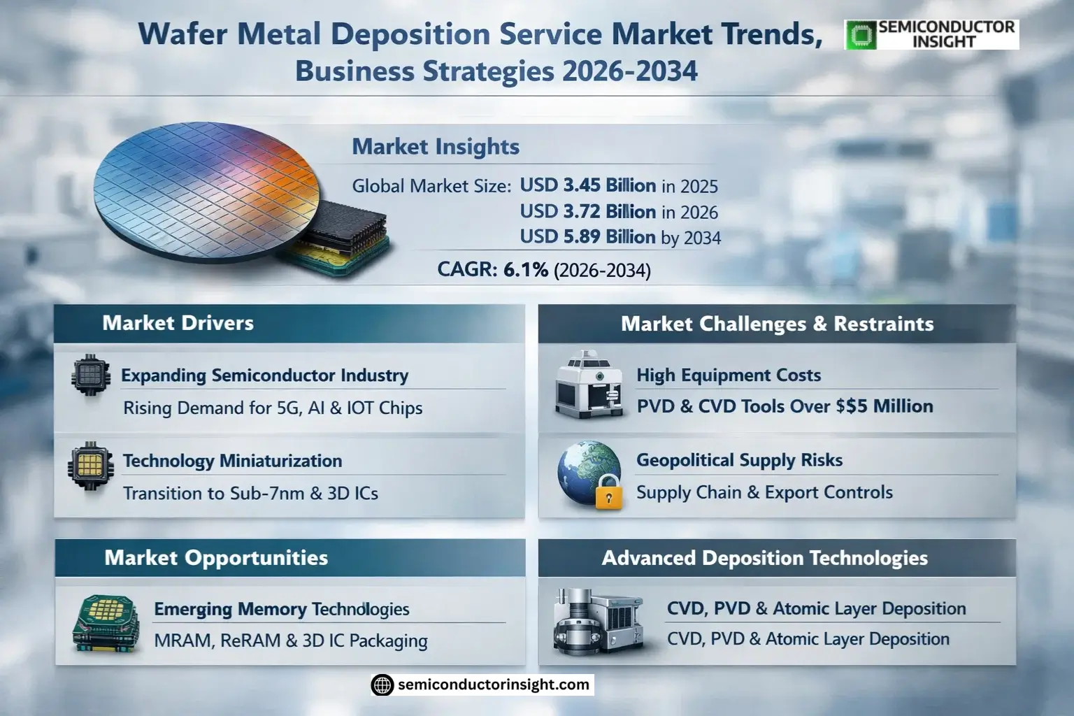
Global Wafer Metal Deposition Service Market size was valued at USD 3.45 billion in 2025. The market is projected to grow from USD 3.72 billion in 2026 to USD 5.89 billion by 2034, exhibiting a CAGR of 6.1% during the forecast period.
Wafer metal deposition services involve thin-film coating processes critical for semiconductor manufacturing, including chemical vapor deposition (CVD) and physical vapor deposition (PVD). These techniques deposit conductive or insulating layers on silicon wafers to create integrated circuits, MEMS devices, and advanced packaging solutions.
The market growth is driven by increasing demand for consumer electronics, automotive semiconductors, and 5G infrastructure. Key players like Platypus Technologies and Vanguard International Semiconductor Corporation are expanding production capacities to meet rising demand for advanced node chips. The shift toward smaller process nodes below 7nm requires more sophisticated deposition technologies, further propelling market expansion.
MARKET DRIVERS
Expanding Semiconductor Industry Demands
Global semiconductor industry, valued at over USD 500 billion, continues to drive demand for wafer metal deposition services. The increasing production of advanced chips for 5G, AI applications, and IoT devices requires precision deposition techniques at nanometer scales, creating steady market growth opportunities for specialized service providers.
Technology Miniaturization Trends
As chip designs shrink below 7nm nodes, wafer metal deposition services must deliver atomic-level precision with materials like copper and tungsten. The transition to 3D chip architectures and advanced packaging solutions further increases the technical requirements for these services.
The shift towards gallium nitride (GaN) and silicon carbide (SiC) semiconductors for power electronics presents new challenges that advanced wafer metal deposition services are uniquely positioned to address.
MARKET CHALLENGES
High Capital Equipment Costs
Establishing and maintaining wafer metal deposition capabilities requires multimillion-dollar investments in physical vapor deposition (PVD) and chemical vapor deposition (CVD) systems. The average cost for a state-of-the-art deposition tool exceeds USD 5 million, creating significant barriers to market entry.
Other Challenges
Material Purity Requirements
Deposition materials must maintain 99.9999% purity levels, with stringent controls on oxygen and moisture content throughout the deposition process.
Process Development Complexity
Each new semiconductor node requires extensive process redevelopment, with deposition parameters needing adjustment for different substrate materials and device architectures.
MARKET RESTRAINTS
Geopolitical Supply Chain Risks
The concentration of wafer metal deposition service providers in specific regions creates vulnerabilities in the semiconductor supply chain. Trade restrictions and export controls on deposition materials like high-purity sputtering targets impact service availability and pricing.
MARKET OPPORTUNITIES
Emerging Memory Technologies
The development of next-generation memory technologies, including MRAM, ReRAM, and PCRAM, creates substantial growth potential for specialized wafer metal deposition services. These technologies require novel material stacks with precise interfacial control that existing deposition techniques can provide.
Packaging Innovation Needs
Advanced packaging approaches like chiplets and 3D IC integration demand new deposition capabilities for through-silicon vias (TSVs) and redistribution layers. Wafer Metal Deposition Service Market stands to benefit from these packaging trends, with projected growth exceeding 15% annually in this segment.
Wafer Metal Deposition Service Market Trends
Advanced Deposition Technologies Gaining Traction
Wafer Metal Deposition Service Market is witnessing accelerated adoption of advanced deposition techniques. Chemical vapor deposition (CVD) and physical vapor deposition (PVD) methods are being refined to achieve higher precision in semiconductor manufacturing. Manufacturers are investing in atomic layer deposition capabilities to meet the growing demand for nanometer-scale accuracy in wafer processing.
Other Trends
Consumer Electronics Driving Demand
The proliferation of smart devices and IoT applications continues to fuel demand for wafer metal deposition services. Leading service providers report a 25% increase in orders from consumer electronics manufacturers seeking high-performance semiconductor components with improved thermal and electrical properties.
Regional Market Specialization Intensifies
Asia-Pacific remains the dominant region for wafer metal deposition services, with China, Japan, and South Korea accounting for over 60% of global capacity. Specialization is emerging by region, with Taiwanese providers focusing on advanced packaging applications while Chinese firms expand in MEMS-related deposition services. European and North American markets are seeing growth in specialty deposition for automotive and industrial applications.
Competition Among Service Providers
Wafer Metal Deposition Service Market features intense competition among established players like Platypus Technologies and newer entrants specializing in niche applications. Market leaders are differentiating through proprietary deposition techniques and partnerships with semiconductor manufacturers to develop customized solutions.
Sustainability Considerations Emerging
Environmental factors are becoming increasingly important in metal deposition processes. Service providers are implementing closed-loop systems for precursor materials and exploring alternatives to traditional deposition chemistries. This trend reflects growing industry attention to process sustainability without compromising deposition quality or throughput.
COMPETITIVE LANDSCAPE
Key Industry Players
Dominant Players and Emerging Challengers in Wafer Deposition Services
Wafer Metal Deposition Service Market is led by established semiconductor equipment providers and specialty coating companies, with Platypus Technologies and Power Master Semiconductor Co., Ltd. holding significant market share. The industry shows moderate concentration with the top five players accounting for approximately 45% of global revenue in 2025. Chemical Vapor Deposition (CVD) remains the dominant technology segment, though Physical Vapor Deposition (PVD) is gaining traction in advanced packaging applications.
Regional specialists like Kyodo International, Inc (Japan) and Vanguard International Semiconductor Corporation (Taiwan) maintain strong positions in Asian markets. Emerging players such as MSE Supplies LLC and Axetris are expanding capabilities to serve the growing demand for MEMS and optoelectronic wafer processing. Joint ventures and technology partnerships are becoming prevalent as companies seek to combine deposition expertise with packaging know-how.
List of Key Wafer Metal Deposition Service Companies Profiled
- Platypus Technologies
- Power Master Semiconductor Co., Ltd.
- JX Advanced Metals Corporation
- Kyodo International, Inc
- Vanguard International Semiconductor Corporation
- PVD Products
- MSE Supplies LLC
- Enzan Factory Co., Ltd.
- PacTech
- Axetris
- OnChip
- Central Semiconductor
- Prosperity Power Technology Inc.
- Integrated Service Technology Inc.
- CHIPBOND Technology Corporation
Segment Analysis:
| Segment Category | Sub-Segments | Key Insights |
| By Type |
|
Chemical Vapor Deposition stands as the dominant segment due to:
|
| By Application |
|
Consumer Electronics leads application segments because:
|
| By End User |
|
Foundries represent the core user segment as:
|
| By Technology Node |
|
Advanced Nodes show strongest demand trends due to:
|
| By Material Type |
|
Copper remains the material of choice as:
|
Regional Analysis: Global Wafer Metal Deposition Service Market
Asia-Pacific
Taiwan’s dominance in semiconductor foundries creates sustained demand for advanced wafer metal deposition services. The concentration of leading-edge logic fabs drives innovation in atomic layer deposition (ALD) and copper interconnect technologies.
China’s multi-billion dollar investments in new fabs are transforming its wafer metal deposition service landscape. Local equipment suppliers are gaining traction, while international deposition service providers establish joint ventures.
South Korea’s memory chip manufacturing requires specialized deposition techniques for 3D NAND and DRAM. The transition to high-aspect-ratio structures and new materials creates unique opportunities for deposition service innovators.
Japan maintains a strong position in deposition equipment manufacturing, directly benefiting wafer metal deposition service providers. Collaboration between material scientists and deposition specialists drives breakthroughs in advanced packaging.
North America
North America remains a key innovation center for wafer metal deposition services, particularly in R&D and specialty applications. The U.S. hosts leading deposition equipment manufacturers and materials science research institutions. Regional demand is driven by advanced logic development, compound semiconductors, and government initiatives to rebuild domestic semiconductor capacity. Major IDMs and fabless companies collaborate closely with deposition service providers to optimize processes for next-generation nodes.
Europe
Europe’s Wafer Metal Deposition Service Market focuses on specialized applications including power semiconductors, MEMS, and automotive chips. The region benefits from strong materials science expertise and precision engineering capabilities. Deposition service providers support Europe’s strategic autonomy initiatives in semiconductor manufacturing. Collaborative R&D projects between equipment suppliers, research institutes, and foundries drive innovations in alternative materials and sustainable deposition processes.
Middle East & Africa
The Middle East is emerging as a potential growth area for wafer metal deposition services through strategic investments in semiconductor manufacturing infrastructure. Government-backed initiatives aim to create localized semiconductor ecosystems. While current demand is limited compared to other regions, long-term projects could establish new centers for deposition technology development, particularly in specialized applications like photonics.
South America
South America’s Wafer Metal Deposition Service Market remains relatively small but shows potential in specific niches. Brazil and Mexico host semiconductor packaging and testing facilities that utilize basic deposition technologies. The region primarily serves as a market for imported deposition equipment rather than a significant service provider location.
Report Scope
This market research report provides a comprehensive analysis of the Global Wafer Metal Deposition Service Market , covering the forecast period 2025-2034. It offers detailed insights into market dynamics, technological advancements, competitive landscape, and key trends shaping the industry.
Key focus areas of the report include:
- Market Overview: The report begins with an overview outlining its current market scenario, key growth indicators, and industry transformation drivers. It discusses macroeconomic factors, demand-supply balance, regulatory landscape, and the strategic role of semiconductor manufacturing in powering advancements across industries such as consumer electronics, communication, automotive, and industrial applications.
- Market Size & Forecast: Historical data and future projections for revenue, unit shipments, and market value across major regions and segments.
- Segmentation Analysis: Detailed breakdown by product type (Chemical Vapor Deposition, Physical Vapor Deposition, Others), application (Consumer Electronics, Communication, Automotive, Others), and end-user industry.
- Regional Insights: Insights into market performance across North America, Europe, Asia-Pacific, South America, and Middle East & Africa, including country-level analysis.
- Competitive Landscape: Profiles of leading market participants, including their product offerings, R&D focus, manufacturing capabilities, and recent developments.
- Technology Trends & Innovation: Assessment of emerging deposition technologies, integration of advanced materials, and evolving industry standards.
- Market Drivers & Restraints: Evaluation of factors driving market growth along with challenges in supply chain, regulatory constraints, and technological barriers.
- Stakeholder Insights: Strategic opportunities for semiconductor manufacturers, equipment suppliers, foundries, and investors.
Primary and secondary research methods are employed, including interviews with industry experts, data from verified sources, and company financial reports to ensure accuracy and reliability of market insights.
FREQUENTLY ASKED QUESTIONS:
What is the current market size of Wafer Metal Deposition Service Market?
-> Wafer Metal Deposition Service Market size was valued at USD 3.45 billion in 2025. The market is projected to grow from USD 3.72 billion in 2026 to USD 5.89 billion by 2034, exhibiting a CAGR of 6.1% during the forecast period.
What are the key segments in the Wafer Metal Deposition Service Market?
-> The market is segmented by:
- Type: Chemical Vapor Deposition (projected to reach USD million by 2034), Physical Vapor Deposition, Others
- Application: Consumer Electronics, Communication, Automotive, Others
Which companies lead the Wafer Metal Deposition Service Market?
-> Key players include Platypus Technologies, Power Master Semiconductor Co., Ltd., JX Advanced Metals Corporation, Vanguard International Semiconductor Corporation, PVD Products, MSE Supplies LLC, PacTech, Axetris, and OnChip, among others. The top five players held approximately % market share in 2025.
What is the regional outlook for this market?
-> The U.S. market was estimated at USD million in 2025, while China is projected to reach USD million. Asia-Pacific shows significant growth potential in wafer metal deposition services.
What are the key application areas driving market growth?
-> Major applications include consumer electronics (smartphones, tablets), communication infrastructure, automotive electronics, and industrial semiconductors, with increasing demand for advanced chip packaging solutions.
Get Sample Report PDF for Exclusive Insights
Report Sample Includes
- Table of Contents
- List of Tables & Figures
- Charts, Research Methodology, and more...
 Download Sample Report PDF