Wafer-level chip-scale package (WLCSP) with copper pillar bump Market Insights
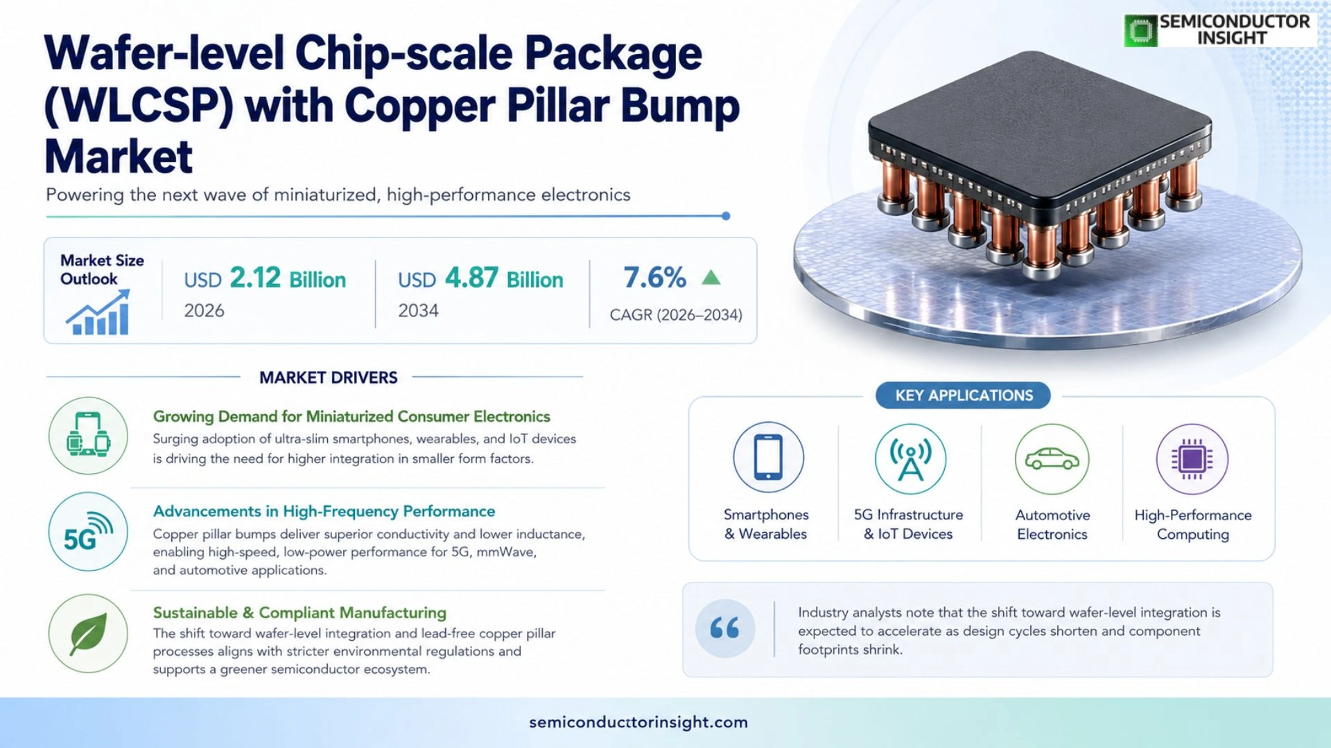
Global Wafer-level chip-scale package (WLCSP) with copper pillar bump market size was valued at USD 2.03 billion in 2025. The market is projected to grow from USD 2.12 billion in 2026 to USD 4.87 billion by 2034, exhibiting a CAGR of 7.6% during the forecast period.
Wafer-level chip-scale package (WLCSP) with copper pillar bump is an advanced semiconductor packaging solution that mounts bare dies directly on a wafer using copper pillars as interconnects. This approach delivers ultra‑thin profiles, superior thermal‑electrical performance, and reduced signal loss, making it ideal for high‑density mobile devices, automotive electronics, and emerging IoT modules.
The market is accelerating because device manufacturers demand higher integration density while shrinking form factors; meanwhile, the rollout of 5G smartphones and autonomous vehicle sensors fuels adoption of WLCSP technology. Furthermore, ongoing R&D investments by leading foundries improve reliability of copper‑pillar interconnects, and strategic collaborations,such as recent joint development programs announced in early 2024 between major packaging firms,are expected to broaden application scope across multiple end‑markets.
MARKET DRIVERS
Growing Demand for Miniaturized Consumer Electronics
Wafer-level chip-scale package (WLCSP) with copper pillar bump Market is being propelled by the rapid adoption of ultra‑slim smartphones, wearables, and IoT sensors. Manufacturers seek higher integration density while maintaining a thin form factor, and WLCSP offers a direct‑die‑to‑carrier solution that eliminates the need for traditional substrate interposers.
Advancements in High‑Frequency Performance
Copper pillar bumps provide superior electrical conductivity and reduced inductance compared with conventional solder bumps, enabling better signal integrity for 5G and mmWave applications. This technical advantage translates into higher data rates and lower power consumption, reinforcing market adoption across telecommunications and automotive sectors.
➤ Industry analysts note that the shift toward wafer‑level integration is expected to accelerate as design cycles shorten and component footprints shrink.
Additionally, the push for environmentally friendly manufacturing,driven by stricter regulations,favours lead‑free copper pillar processes, further cementing the strategic relevance of the WLCSP platform.
MARKET CHALLENGES
Manufacturing Complexity and Yield Management
Implementing copper pillar technology requires precise control of electroplating, planarization, and reflow steps. Any variation can lead to defectivity that directly impacts wafer yield, raising concerns for high‑volume producers.
Other Challenges
Cost Sensitivity
The capital expense associated with retrofitting fab lines for copper pillar bumping can be substantial. While performance gains are clear, price‑sensitive segments such as low‑cost wearables may experience slower adoption rates.
MARKET RESTRAINTS
Limited Equipment Availability
Specialized copper pillar deposition tools are produced by a small number of vendors, creating a bottleneck for fabs seeking rapid scale‑up. This scarcity can delay project timelines and increase lead times for component qualification.
MARKET OPPORTUNITIES
Emerging Applications in 5G, Automotive, and AI Edge
The convergence of 5G infrastructure, advanced driver‑assistance systems, and AI‑enabled edge devices fuels demand for high‑performance, low‑profile packaging. WLCSP with copper pillar bumps offers the thermal management and electrical performance required for these next‑generation applications, opening significant growth pathways for early adopters.
Wafer-level chip-scale package (WLCSP) with copper pillar bump Market Trends
Growth Driven by 5G Mobile and Automotive Sensor Adoption
Wafer-level chip-scale package (WLCSP) with copper pillar bump Market is experiencing a clear acceleration as device manufacturers seek higher integration density while reducing package footprints. The rollout of 5G smartphones has created a demand for ultra‑thin, high‑performance interconnects that can handle increased data rates with minimal signal loss. At the same time, autonomous‑vehicle sensor systems require robust thermal‑electrical performance in compact form factors, making copper‑pillar interconnects an attractive solution. These twin forces are prompting foundries and packaging firms to prioritize WLCSP technologies in their roadmaps, resulting in a noticeable shift toward wafer‑level integration across multiple high‑growth segments.
Other Trends
Advancements in Copper Pillar Reliability
Recent R&D investments have focused on improving the mechanical stability and lifespan of copper pillars. Process refinements such as optimized electro‑plating, barrier‑layer engineering, and stress‑relief annealing have reduced crack propagation and delamination risks. Collaborative development programs announced in early 2024 between leading packaging providers and semiconductor manufacturers have accelerated the qualification of next‑generation copper‑pillar designs, enabling broader adoption in temperature‑sensitive automotive and industrial applications.
Expansion into IoT and Edge‑Computing Modules
Beyond mobile and automotive, the Wafer-level chip-scale package (WLCSP) with copper pillar bump Market is gaining traction in Internet‑of‑Things (IoT) and edge‑computing devices. These applications benefit from the package’s ultra‑thin profile, which facilitates integration into space‑constrained wearables, smart sensors, and compact edge AI modules. The inherent low‑inductance and high‑frequency performance of copper pillars support the stringent power‑efficiency and latency requirements of edge workloads. As edge deployments increase globally, manufacturers are leveraging the scalability of wafer‑level processes to meet volume demands while maintaining cost effectiveness.
COMPETITIVE LANDSCAPE
Key Industry Players
Wafer-level chip-scale package (WLCSP) with copper pillar bump – Competitive Overview
WLCSP market with copper‑pillar bump is currently led by a handful of large packaging conglomerates that combine front‑end foundry capabilities with advanced back‑end assembly. ASE Technology Holding, Amkor Technology, and JCET Group together command over 45 % of global capacity, leveraging their extensive R&D pipelines and multi‑layer copper‑pillar processes to secure design‑wins in premium smartphones and automotive sensor modules. Their breadth of service,from wafer‑level fan‑out redistribution to post‑die thinning,creates a high entry barrier, while strategic alliances with leading fab sites (e.g., TSMC’s CoWoS platform) further consolidate their market dominance.
Niche but technically potent players such as Siliconware Precision Industries (SPIL), UTAC Holdings, Samsung Electro‑Mechanics, and Powertech Technology (PTI) differentiate through specialized copper‑pillar bump engineering, ultra‑thin profile optimization, and targeted collaborations with IoT and 5G chipset designers. These firms often focus on specific end‑markets,high‑frequency RF modules, autonomous‑vehicle sensors, and wearables,where reliability and miniaturization are paramount. The competitive landscape remains dynamic, with joint development programs announced in early 2024 accelerating technology transfer and expanding the addressable market for copper‑pillar‑based WLCSP solutions.
List of Key Wafer-level Chip-Scale Package (WLCSP) with Copper Pillar Bump Companies Profiled
- ASE Technology Holding Co., Ltd.
- Amkor Technology, Inc.
- JCET Group Co., Ltd.
- Siliconware Precision Industries Co., Ltd. (SPIL)
- Samsung Electro‑Mechanics Co., Ltd.
- UTAC Holdings Ltd.
- TSMC – Advanced Packaging Division
- Powertech Technology Inc. (PTI)
- ChipMOS Technologies Inc.
- STATS ChipPAC (integrated within JCET)
- Infineon Technologies AG – Packaging Solutions
- Taiwan Semiconductor Manufacturing Co.
Segment Analysis:
| Segment Category | Sub-Segments | Key Insights |
| By Type |
|
Copper Pillar Bump
|
| By Application |
|
Smartphone Integration
|
| By End User |
|
Device Manufacturers
|
| By Integration Density |
|
High‑Density Integration
|
| By Performance Requirement |
|
Thermal Management Focus
|
Regional Analysis: North America
The automotive sector is increasingly integrating sophisticated electronic systems, driving demand for compact and high-reliability WLCSP with copper pillar bump solutions for applications like ADAS and electric vehicle components.
The consumer electronics industry continues to seek smaller, more powerful components for smartphones, wearables, and other devices, making WLCSP with copper pillar bump a preferred choice for achieving miniaturization and enhanced performance.
The industrial automation sector benefits from the reliability and performance of WLCSP with copper pillar bump in controlling systems and embedded applications, contributing to increased efficiency and precision.
The aerospace and defense industries leverage the robustness and high-reliability characteristics of WLCSP with copper pillar bump for critical electronic systems operating in demanding environments.
Europe
Europe presents a significant market for Wafer-level chip-scale package (WLCSP) with copper pillar bump, driven by strong industrial sectors and a growing emphasis on advanced electronics. Key applications include automotive, industrial automation, and consumer electronics. The region’s focus on energy efficiency and sustainable technologies is also creating new opportunities for this technology.
Asia-Pacific
Asia-Pacific is a rapidly expanding market for WLCSP with copper pillar bump, fueled by the robust growth of the electronics manufacturing industry in countries like China, Japan, and South Korea. The region’s dominance in consumer electronics production and the increasing adoption of advanced automotive technologies are key growth drivers.
South America
South America exhibits a growing demand for WLCSP with copper pillar bump, particularly in the consumer electronics and industrial sectors. The expansion of manufacturing capabilities and increasing disposable incomes are contributing to this growth.
Middle East & Africa
The Middle East & Africa region represents a smaller but emerging market for WLCSP with copper pillar bump. The growth is primarily driven by investments in infrastructure development, telecommunications, and a rising consumer electronics market.
Report Scope
This market research report provides a comprehensive analysis of the Wafer-level chip-scale package (WLCSP) with copper pillar bump Market , covering the forecast period 2026–2034. It offers detailed insights into market dynamics, technological advancements, competitive landscape, and key trends shaping the industry.
Key focus areas of the report include:
- Market Overview: The report begins with an overview outlining its current market scenario, key growth indicators, and industry transformation drivers. It discusses macroeconomic factors, demand–supply balance, regulatory landscape, and the strategic role of semiconductors in powering advancements across industries such as automotive, telecommunications, consumer electronics, and industrial automation.
- Market Size & Forecast: Historical data and future projections for revenue, unit shipments, and market value across major regions and segments.
- Segmentation Analysis: Detailed breakdown by product type, technology, application, and end-user industry to identify high-growth segments and investment opportunities.
- Regional Insights: Insights into market performance across North America, Europe, Asia-Pacific, Latin America, and the Middle East & Africa, including country-level analysis where relevant.
- Competitive Landscape: Profiles of leading market participants, including their product offerings, R&D focus, manufacturing capacity, pricing strategies, and recent developments such as mergers, acquisitions, and partnerships.
- Technology Trends & Innovation: Assessment of emerging technologies, integration of AI/IoT, semiconductor design trends, fabrication techniques, and evolving industry standards.
- Market Drivers & Restraints: Evaluation of factors driving market growth along with challenges, supply chain constraints, regulatory issues, and market-entry barriers.
- Stakeholder Insights: Insights for component suppliers, OEMs, system integrators, investors, and policymakers regarding the evolving ecosystem and strategic opportunities.
Primary and secondary research methods are employed, including interviews with industry experts, data from verified sources, and real-time market intelligence to ensure the accuracy and reliability of the insights presented.
FREQUENTLY ASKED QUESTIONS:
What is the current market size of Wafer-level chip-scale package (WLCSP) with copper pillar bump Market?
-> Wafer-level chip-scale package (WLCSP) with copper pillar bump Market was valued at USD 2.03 billion in 2025 and is expected to reach USD 4.87 billion by 2034.
Which key companies operate in Wafer-level chip-scale package (WLCSP) with copper pillar bump Market?
-> Key players include ASE Technology Holding, Amkor Technology, JCET Group, STATS ChipPAC, TSMC, and other leading semiconductor packaging firms.
What are the key growth drivers?
-> Key growth drivers include the proliferation of 5G smartphones, automotive advanced driver‑assistance systems (ADAS), increasing IoT device density, and the demand for ultra‑thin, high‑performance packaging solutions.
Which region dominates the market?
-> Asia-Pacific leads the market, driven by high manufacturing capacity in China, Taiwan, South Korea, and Japan, while North America and Europe also show strong demand.
What are the emerging trends?
-> Emerging trends include advanced heterogeneous integration, fan‑out wafer‑level interconnects, AI‑assisted design optimization, and the expansion of WLCSP into automotive and edge‑computing applications.
Get Sample Report PDF for Exclusive Insights
Report Sample Includes
- Table of Contents
- List of Tables & Figures
- Charts, Research Methodology, and more...


