
MARKET INSIGHTS
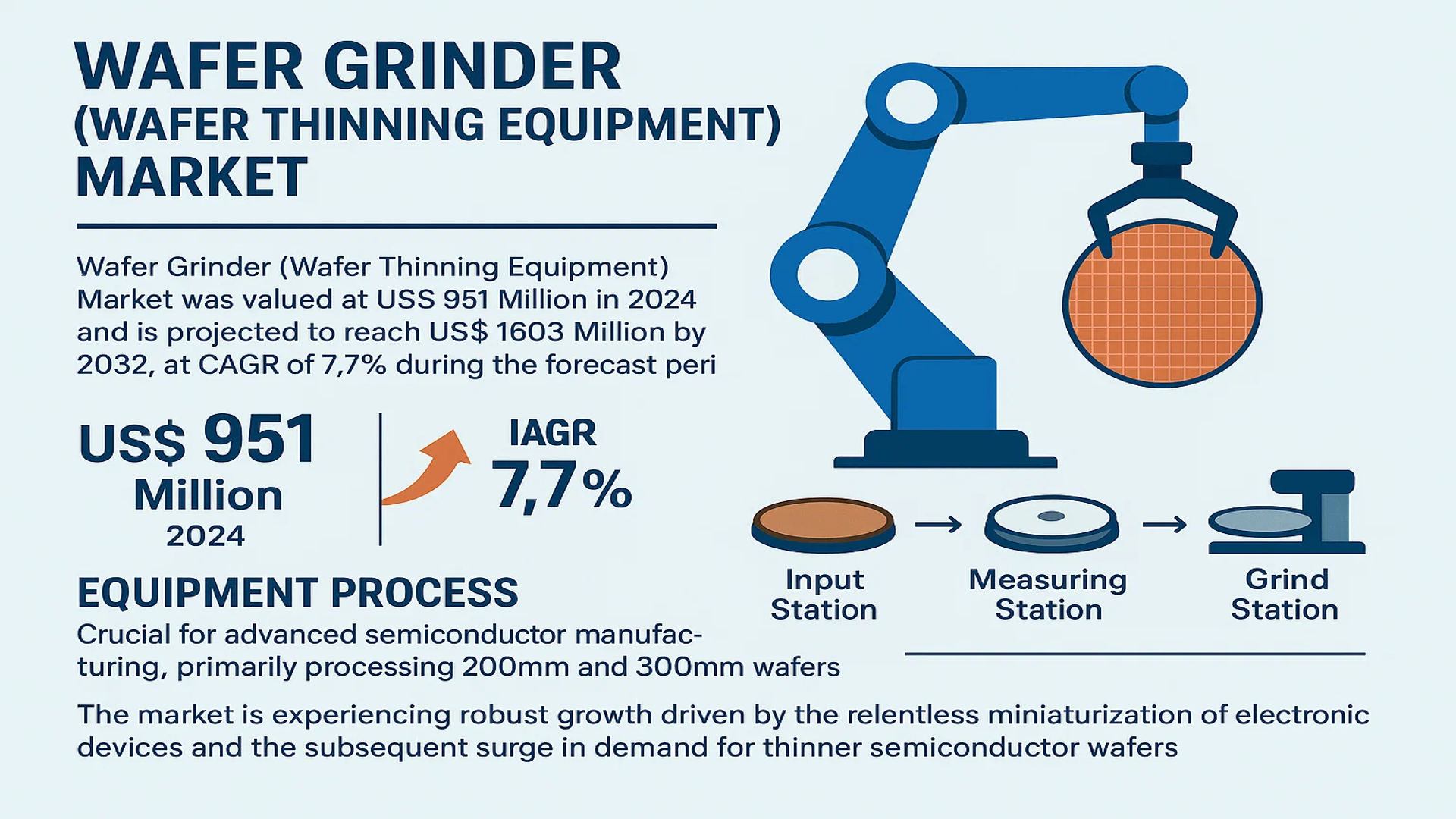
The global Wafer Grinder (Wafer Thinning Equipment) Market was valued at 951 million in 2024 and is projected to reach US$ 1603 million by 2032, at a CAGR of 7.7% during the forecast period.
Wafer Grinder (Wafer Thinning Equipment) uses a centrally located robot to move a wafer from an input station to a measuring station. Thereafter, the wafer is moved into a grind station and a wash station sequentially. This equipment is crucial for achieving the precise thickness required in advanced semiconductor manufacturing, primarily for processing 200mm and 300mm wafers.
The market is experiencing robust growth driven by the relentless miniaturization of electronic devices and the subsequent surge in demand for thinner semiconductor wafers. The processing of 300mm wafers dominates the application segment, accounting for approximately 83% of global demand, because larger wafers allow for higher production yields and reduced manufacturing costs per chip. Furthermore, fully automatic systems lead the market by automation level, holding a 52% share, as they offer superior precision and efficiency for high-volume production. Geographically, the Asia-Pacific (APAC) region is the largest consumer, representing about 78% of the global market, fueled by its dominant semiconductor manufacturing ecosystem. Key players such as Disco, TOKYO SEIMITSU, and Okamoto Semiconductor Equipment Division collectively account for a significant portion of the market revenue.
MARKET DYNAMICS
MARKET DRIVERS
Technological Advancements in Semiconductor Manufacturing to Drive Market Growth
The semiconductor industry is undergoing rapid technological evolution, driven by the relentless demand for smaller, more powerful, and energy-efficient electronic devices. This progression necessitates increasingly thinner and more precisely engineered wafers, which directly fuels the demand for high-performance wafer thinning equipment. Advanced wafer grinders are critical for achieving the sub-100-micron thicknesses required for modern 3D IC packaging and advanced memory chips. The shift towards more complex node architectures, such as those below 7nm, places unprecedented emphasis on thinning precision to maintain structural integrity and electrical performance. This technological arms race in semiconductor fabrication is a primary catalyst for innovation and adoption in the wafer grinding equipment market, as manufacturers continuously seek solutions that offer superior accuracy, higher throughput, and reduced yield loss.
Surge in 300mm Wafer Demand to Boost Market Expansion
The dominance of 300mm wafers in semiconductor manufacturing is a monumental driver for the wafer grinder market. Accounting for approximately 83% of global demand, 300mm wafers offer significant economies of scale by allowing more chips to be produced per wafer, drastically reducing the cost per die. This trend is intensifying as leading-edge logic and memory production is almost exclusively based on this larger format. The fabrication of these wafers requires highly specialized thinning equipment capable of handling their size and weight while maintaining nanometric-level precision across the entire surface. The capital expenditure directed towards new 300mm fabrication facilities, particularly across Asia, represents a sustained and powerful source of demand for advanced wafer grinding systems, ensuring robust market growth for the foreseeable future.
Proliferation of IoT and Automotive Electronics to Fuel Equipment Adoption
The explosive growth of the Internet of Things (IoT) and the increasing electrification of automobiles are creating substantial downstream demand for semiconductors, which in turn drives the wafer thinning equipment market. IoT devices, ranging from smart sensors to wearable technology, require ultra-compact and low-power chips, which are enabled by thin wafers. Similarly, modern vehicles incorporate hundreds of semiconductors for everything from infotainment systems to advanced driver-assistance systems (ADAS) and powertrain control. These applications often demand robust chips capable of operating in harsh environments, a requirement met by thinning and subsequent processes like backside metallization. This diversification and growth in end-market applications provide a broad and stable foundation for continued investment in wafer grinding capabilities across the supply chain.
Furthermore, the strategic focus of national governments on achieving semiconductor self-sufficiency and bolstering domestic chip production is accelerating investments in manufacturing infrastructure, thereby propelling the demand for essential equipment like wafer grinders.
➤ For instance, major global initiatives are channeling hundreds of billions of dollars into semiconductor manufacturing capacity, directly increasing the addressable market for wafer thinning equipment suppliers.
Moreover, the ongoing transition towards fully automated grinding systems, which enhance throughput and reduce human error, is anticipated to be a persistent driver throughout the forecast period.
MARKET CHALLENGES
High Capital and Operational Expenditure Poses a Significant Challenge to Market Penetration
While the market is on a strong growth trajectory, the substantial financial investment required for advanced wafer grinding systems presents a formidable challenge. A single state-of-the-art, fully automatic wafer grinder can represent a multi-million-dollar capital investment. This high entry cost is particularly prohibitive for smaller semiconductor fabricators, emerging foundries, and research institutions with limited budgets. Beyond the initial purchase price, operational expenditures contribute significantly to the total cost of ownership. These systems consume substantial amounts of ultra-pure water and specialized chemicals for the cleaning and cooling processes. Furthermore, they require expensive diamond grinding wheels that need regular dressing and replacement to maintain cutting performance and surface quality, adding recurring costs that can strain operational budgets and impact overall profitability for smaller players.
Other Challenges
Yield Management and Process Control
Maintaining high yield rates is a perpetual challenge in wafer thinning. The process can induce micro-cracks, chipping, and subsurface damage that may not be detected until later fabrication stages, leading to costly scrap. Achieving consistent thickness uniformity, especially across the entire 300mm wafer surface, requires exquisite control of grinding parameters and real-time metrology. Any deviation can result in wafer warpage or breakage, particularly when handling ultra-thin wafers below 50 microns, directly impacting production efficiency and cost.
Rapid Technological Obsolescence
The pace of innovation in semiconductor manufacturing means that production equipment can become obsolete relatively quickly. Manufacturers of wafer grinding equipment must continuously invest in research and development to keep their systems compatible with new materials, larger wafer sizes, and more stringent precision requirements. For equipment buyers, this creates a dilemma: investing in a cutting-edge system risks rapid obsolescence, while opting for older technology may compromise competitiveness. This cycle of innovation shortens the effective lifespan of equipment and challenges the return on investment calculations for procurement teams.
MARKET RESTRAINTS
Technical Complexity and Skilled Labor Shortage to Deter Market Growth
Fully automatic wafer grinding systems are marvels of engineering integration, combining precision mechanics, advanced robotics, fluid handling, and sophisticated software control. However, this very complexity acts as a significant restraint on market growth. Operating, programming, and maintaining these systems requires a highly specialized skill set that blends mechanical engineering, mechatronics, and process engineering knowledge. The global semiconductor industry is currently experiencing a well-documented shortage of such skilled technicians and engineers. This talent gap is exacerbated by the concentration of manufacturing expertise in specific geographic hubs, making it difficult for new facilities or those in developing regions to recruit and retain the necessary personnel. Without adequate skilled staffing, companies cannot maximize equipment uptime or troubleshoot complex process issues effectively, leading to lower productivity and potentially deterring investment in the most advanced grinding solutions.
Additionally, the integration of these complex systems into existing fabrication line workflows can be disruptive and time-consuming, requiring extensive calibration and software interfacing to ensure seamless automation, which can temporarily hamper overall production output.
Furthermore, the need for continuous training to keep pace with software updates and new process techniques adds another layer of operational complexity and cost, acting as a subtle but persistent restraint on the broader adoption of the latest equipment generations.
MARKET OPPORTUNITIES
Emergence of Advanced Packaging and Heterogeneous Integration to Unlock New Growth Avenues
The paradigm shift towards advanced packaging techniques, such as 2.5D and 3D IC integration, presents a profound opportunity for the wafer thinning equipment market. These packaging methods, essential for continuing Moore’s Law, involve stacking multiple thin dies vertically, which requires wafers to be thinned to extreme dimensions—often below 50 microns—with exceptional surface quality and mechanical strength. This creates a new tier of performance requirements that current grinding technologies must evolve to meet. The development of ultra-precision grinding solutions capable of handling these fragile, ultra-thin wafers without inducing damage is a key frontier for innovation. Companies that can pioneer grinding and handling technologies for this next generation of packaging will capture a significant and high-value segment of the market, driven by the demand for high-bandwidth memory, AI accelerators, and other performance-intensive applications.
Additionally, the exploration of new substrate materials beyond silicon, such as silicon carbide (SiC) and gallium nitride (GaN) for power electronics and RF applications, requires the adaptation of grinding processes. These materials are harder and more brittle than silicon, presenting unique machining challenges.
Furthermore, the increasing strategic investments in compound semiconductor manufacturing open a parallel growth path for equipment suppliers who can develop specialized solutions for these demanding materials, thereby diversifying their market reach and reducing reliance on the traditional silicon cycle.
WAFER GRINDER (WAFER THINNING EQUIPMENT) MARKET TRENDS
Advancements in Automation and Precision to Emerge as a Trend in the Market
The global semiconductor industry’s relentless pursuit of miniaturization and performance is fundamentally reshaping the wafer thinning equipment landscape. A dominant trend is the accelerated shift towards fully automated grinding systems, which currently command over 52% of the global market share. This transition is driven by the critical need for enhanced precision, superior yield management, and reduced human-induced variability in high-volume manufacturing environments. Recent technological innovations focus on integrating advanced in-process metrology and real-time thickness monitoring systems, allowing for closed-loop control during the grinding process. This ensures that wafers are thinned to tolerances of less than 10 micrometers with exceptional surface integrity, which is paramount for advanced 3D packaging and stacking applications like High Bandwidth Memory (HBM). Furthermore, equipment manufacturers are increasingly incorporating AI-driven predictive maintenance algorithms to minimize unplanned downtime and optimize consumable usage, thereby improving overall equipment effectiveness (OEE) in fab operations.
Other Trends
Expansion of 300mm Wafer Processing
The market is experiencing a pronounced expansion in demand for equipment capable of processing 300mm wafers, which now account for approximately 83% of global application demand. This surge is intrinsically linked to the economics of semiconductor manufacturing, as larger wafers allow for a significantly higher number of dies per wafer, drastically reducing the cost per chip. However, thinning these larger substrates introduces substantial technical challenges, including increased risks of warpage and stress-induced defects. Consequently, equipment evolution is characterized by the development of more robust chucking systems, advanced stress-relief grinding techniques, and multi-step processes that combine coarse grinding with fine polishing. This trend is most visible in the Asia-Pacific region, where leading-edge logic and memory fabs are scaling production capacity to meet the insatiable demand for components used in data centers, artificial intelligence accelerators, and next-generation mobile devices.
Growing Adoption in Power Semiconductor and Compound Semiconductor Manufacturing
Beyond traditional silicon-based ICs, a significant growth vector for wafer thinning equipment is its increasing adoption in the manufacturing of power devices and compound semiconductors. Materials such as silicon carbide (SiC) and gallium nitride (GaN) are essential for high-efficiency, high-power applications in electric vehicles, renewable energy systems, and 5G infrastructure. These materials are notoriously hard and brittle, presenting unique challenges for the thinning process without introducing micro-cracks or sub-surface damage. This has catalyzed the development of specialized grinding wheels with diamond abrasives, optimized coolants, and tailored process recipes that ensure the structural integrity of these delicate wafers. The market for equipment dedicated to these materials is growing at an accelerated pace, reflecting the broader industrial shift towards electrification and energy efficiency, and is opening new revenue streams for equipment manufacturers who can master these complex material requirements.
COMPETITIVE LANDSCAPE
Key Industry Players
Leading Manufacturers Focus on Technological Innovation and Regional Expansion to Secure Market Position
The global Wafer Grinder (Wafer Thinning Equipment) market exhibits a highly concentrated competitive structure, dominated by a handful of established players who collectively command approximately 90% of the revenue share as of 2024. This concentration is primarily due to the significant technological barriers to entry and the substantial capital investment required for research, development, and manufacturing of these precision systems. The market’s epicenter is firmly rooted in the Asia-Pacific region, which consumes about 78% of global output, compelling key players to maintain a strong operational footprint in semiconductor hubs like Japan, South Korea, and Taiwan.
Disco Corporation and TOKYO SEIMITSU are unequivocal leaders in this space. Their dominance is not merely a function of market share but is built upon decades of specialized engineering expertise, extensive patent portfolios, and deep, trust-based relationships with major semiconductor fabrication plants (fabs). These companies are at the forefront of developing fully automatic systems, which constitute over half of the market, by integrating advanced robotics, real-time metrology, and AI-driven process control to achieve unparalleled precision in wafer thinning, a critical step for advanced 3D packaging and memory devices.
Meanwhile, other significant players like Okamoto Semiconductor Equipment Division and G&N are strengthening their positions through strategic initiatives. This includes heavy investment in R&D to enhance grinding speed and yield while minimizing sub-surface damage, a key concern for manufacturers. Furthermore, companies are pursuing geographical expansion strategies, particularly into emerging semiconductor manufacturing locales in Southeast Asia and North America, to capture new growth opportunities beyond their traditional strongholds.
While the market is top-heavy, smaller and specialized firms such as Revasum and CETC are carving out niches. They compete by offering cost-effective solutions for specific applications or by providing exceptional technical support and service, which are highly valued by smaller fab operations. However, the overall competitive dynamics are shaped by the technological roadmaps of the largest semiconductor manufacturers, whose relentless pursuit of thinner wafers and higher throughput continuously raises the performance bar for all equipment suppliers.
List of Key Wafer Grinder (Wafer Thinning Equipment) Companies Profiled
- Disco Corporation (Japan)
- TOKYO SEIMITSU CO., LTD. (Japan)
- Okamoto Semiconductor Equipment Division (Japan)
- G&N Genauigkeitsschleiftechnik Nürnberg GmbH (Germany)
- China Electronics Technology Group Corporation (CETC) (China)
- Koyo Machinery Industries Co., Ltd. (Japan)
- Revasum, Inc. (U.S.)
- WAIDA MFG. CO., LTD. (Japan)
- Hunan Yujing Machine Industrial Co., Ltd. (China)
- SpeedFam (Japan)
Segment Analysis:
By Level of Automation
Fully Automatic Segment Dominates the Market Due to Superior Precision and High Throughput
The market is segmented based on level of automation into:
- Fully Automatic
- Semi-Automatic
By Application
300mm Wafer Segment Leads Due to High Demand in Advanced Semiconductor Manufacturing
The market is segmented based on application into:
- 200mm Wafer
- 300mm Wafer
- Others
By End User
Semiconductor Foundries Segment Leads Due to High-Volume Production Requirements
The market is segmented based on end user into:
- Semiconductor Foundries
- Integrated Device Manufacturers (IDMs)
- Research and Development Institutions
By Technology
Grind-Etch Segment Leads Due to its Superior Surface Finish and Damage Control
The market is segmented based on technology into:
- Grind-Etch
- Grind-Polish
- Grind-Tape
Regional Analysis: Wafer Grinder (Wafer Thinning Equipment) Market
Asia-Pacific
The Asia-Pacific region dominates the global Wafer Grinder market, accounting for approximately 78% of global consumption. This leadership position stems from the region’s robust semiconductor manufacturing ecosystem, particularly in China, Japan, South Korea, and Taiwan. These countries are home to major foundries and IDMs (Integrated Device Manufacturers) that require high-volume, precision wafer thinning equipment to support advanced node production. The relentless drive towards miniaturization in consumer electronics and the proliferation of IoT devices fuel continuous capital expenditure in this sector. While the market is mature in established semiconductor hubs like Taiwan and South Korea, China represents a significant growth engine due to substantial government and private investments aimed at achieving semiconductor self-sufficiency. The demand is overwhelmingly for fully automatic systems handling 300mm wafers, which align with the high-throughput requirements of modern fabs.
North America
North America holds a significant, though smaller, share of the Wafer Grinder market, characterized by a focus on research, development, and high-value manufacturing. The region’s market is driven by leading-edge semiconductor companies and R&D institutions that demand equipment capable of extreme precision for next-generation chips, including those for AI, high-performance computing, and advanced automotive applications. Investments from initiatives like the U.S. CHIPS and Science Act, which allocates billions in funding for domestic semiconductor production, are poised to stimulate demand for advanced manufacturing equipment, including wafer thinning systems. However, adoption can be tempered by the high initial investment required for top-tier automated systems, making the market more selective and focused on equipment that offers superior technical capabilities and reliability.
Europe
Europe’s market for Wafer Grinder equipment is steady, supported by a strong automotive industrial base and strategic initiatives like the European Chips Act. The region’s demand is primarily for equipment used in manufacturing power semiconductors, sensors, and microcontrollers for the automotive and industrial sectors. European semiconductor manufacturers often prioritize quality, precision, and long-term equipment reliability, aligning with the performance of fully automatic grinders from established suppliers. While the volume of consumption is lower than in Asia-Pacific, the region remains a critical market for high-value, specialized equipment. The presence of major automotive OEMs and a growing focus on electric vehicles present a stable, long-term demand driver for the semiconductor components that require thinning processes.
South America
The Wafer Grinder market in South America is nascent and represents a minor share of the global total. The region’s semiconductor manufacturing infrastructure is limited, with most demand stemming from a small number of assembly and test facilities rather than advanced front-end fabs. Economic volatility and inconsistent industrial policy have historically limited large-scale investments in capital-intensive semiconductor manufacturing equipment. Consequently, demand is primarily for more cost-sensitive, semi-automatic or refurbished systems rather than the latest fully automated platforms. While long-term growth potential exists as part of broader regional economic development plans, the market currently faces significant challenges related to funding, technical expertise, and infrastructure.
Middle East & Africa
The market in the Middle East & Africa is in its earliest stages of development. Current demand is negligible on a global scale and is primarily met through imports for specific industrial or research applications. There is no significant local semiconductor fabrication ecosystem to drive consistent demand for wafer thinning equipment. Long-term market development is contingent upon major economic diversification efforts and substantial foreign direct investment into technology and manufacturing sectors. Until such foundational investments are made, the region will remain a peripheral market for Wafer Grinder equipment, with growth potential being highly speculative and dependent on large-scale, government-led initiatives.
Report Scope
This market research report provides a comprehensive analysis of the global and regional Wafer Grinder (Wafer Thinning Equipment) markets, covering the forecast period 2025–2032. It offers detailed insights into market dynamics, technological advancements, competitive landscape, and key trends shaping the industry.
Key focus areas of the report include:
- Market Size & Forecast: Historical data and future projections for revenue, unit shipments, and market value across major regions and segments.
- Segmentation Analysis: Detailed breakdown by product type, technology, application, and end-user industry to identify high-growth segments and investment opportunities.
- Regional Outlook: Insights into market performance across North America, Europe, Asia-Pacific, Latin America, and the Middle East & Africa, including country-level analysis where relevant.
- Competitive Landscape: Profiles of leading market participants, including their product offerings, R&D focus, manufacturing capacity, pricing strategies, and recent developments such as mergers, acquisitions, and partnerships.
- Technology Trends & Innovation: Assessment of emerging technologies, integration of AI/IoT, semiconductor design trends, fabrication techniques, and evolving industry standards.
- Market Drivers & Restraints: Evaluation of factors driving market growth along with challenges, supply chain constraints, regulatory issues, and market-entry barriers.
- Stakeholder Analysis: Insights for component suppliers, OEMs, system integrators, investors, and policymakers regarding the evolving ecosystem and strategic opportunities.
Primary and secondary research methods are employed, including interviews with industry experts, data from verified sources, and real-time market intelligence to ensure the accuracy and reliability of the insights presented.
FREQUENTLY ASKED QUESTIONS:
What is the current market size of Global Wafer Grinder (Wafer Thinning Equipment) Market?
-> Wafer Grinder (Wafer Thinning Equipment) Market was valued at 951 million in 2024 and is projected to reach US$ 1603 million by 2032, at a CAGR of 7.7% during the forecast period.
Which key companies operate in Global Wafer Grinder (Wafer Thinning Equipment) Market?
-> Key players include Disco, TOKYO SEIMITSU, G&N, Okamoto Semiconductor Equipment Division, and CETC, which collectively hold approximately 90% of the global revenue market share.
What are the key growth drivers?
-> Key growth drivers include technological advancements in semiconductor manufacturing, miniaturization of electronic devices, surge in semiconductor demand, growth in 300mm wafer processing, and the shift towards fully automated solutions.
Which region dominates the market?
-> Asia-Pacific is the dominant region, accounting for approximately 78% of global consumption, driven by major semiconductor manufacturing hubs in China, Japan, South Korea, and Taiwan.
What are the emerging trends?
-> Emerging trends include increased adoption of fully automatic systems (holding 52% market share), focus on precision for 300mm wafers (83% of application demand), and integration of advanced robotics and AI for enhanced operational efficiency.

Get Sample Report PDF for Exclusive Insights
Report Sample Includes
- Table of Contents
- List of Tables & Figures
- Charts, Research Methodology, and more...




