
Market Insights
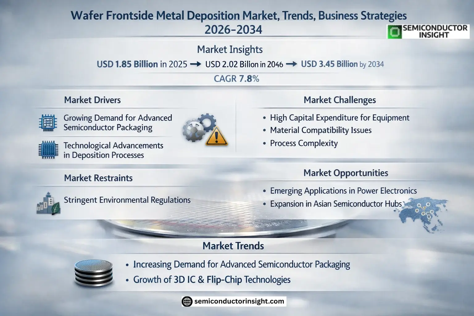
Global Wafer Frontside Metal Deposition Market size was valued at USD 1.85 billion in 2025. The market is projected to grow from USD 2.02 billion in 2026 to USD 3.45 billion by 2034, exhibiting a CAGR of 7.8% during the forecast period.
Wafer frontside metal deposition is a critical semiconductor manufacturing process that involves depositing thin metal layers on the front surface of silicon wafers to create electrical interconnects and contacts. This technology utilizes methods such as electro-less plating, evaporation plating, and sputtering to achieve precise metallization for integrated circuits (ICs) and microelectronic devices.
The market growth is driven by increasing demand for advanced semiconductor packaging, miniaturization of electronic components, and the proliferation of IoT devices. While electro-less plating dominates due to its uniform coating capabilities, emerging applications in automotive electronics and 5G infrastructure are accelerating adoption. Key players like Power Master Semiconductor Co., Ltd. and JX Advanced Metals Corporation are investing in R&D to enhance deposition techniques for next-generation chips.
MARKET DRIVERS
Growing Demand for Advanced Semiconductor Packaging
Wafer Frontside Metal Deposition Market is witnessing significant growth due to increasing demand for advanced semiconductor packaging solutions. With the rise of AI, 5G, and IoT applications, manufacturers require high-performance metal deposition techniques to ensure superior conductivity and miniaturization in chip designs.
Technological Advancements in Deposition Processes
Innovations in atomic layer deposition (ALD) and physical vapor deposition (PVD) techniques are enhancing the precision of wafer frontside metal deposition. These advancements enable better control over thin-film uniformity, crucial for next-generation semiconductor devices.
Additionally, the shift toward 3D IC packaging and fan-out wafer-level packaging (FOWLP) is creating new opportunities for specialized deposition technologies.
MARKET CHALLENGES
High Capital Expenditure for Equipment
Wafer Frontside Metal Deposition Market process requires sophisticated equipment with high precision, leading to substantial capital investment. This acts as a barrier for smaller semiconductor manufacturers entering the market.
Other Challenges
Material Compatibility Issues
Developing deposition materials that adhere to stringent thermal and electrical requirements while maintaining compatibility with evolving wafer materials remains a key challenge.
Process Complexity
Achieving uniform deposition across increasingly larger wafer sizes (300mm+) demands precise control mechanisms, adding to operational complexities.
MARKET RESTRAINTS
Stringent Environmental Regulations
Environmental concerns surrounding the use of certain metals and chemicals in deposition processes are leading to stricter regulations, potentially limiting material choices and increasing compliance costs for wafer frontside metal deposition manufacturers.
MARKET OPPORTUNITIES
Emerging Applications in Power Electronics
The growing adoption of gallium nitride (GaN) and silicon carbide (SiC) semiconductors for power electronics presents significant opportunities for specialized wafer frontside metal deposition solutions that can withstand high temperatures and voltages.
Expansion in Asian Semiconductor Hubs
With semiconductor manufacturing rapidly expanding in Asia-Pacific regions, particularly in China and Taiwan, there is substantial potential for wafer frontside metal deposition equipment and service providers to establish stronger regional presence.
Wafer Frontside Metal Deposition Market Trends
Increasing Demand for Advanced Semiconductor Packaging
Wafer Frontside Metal Deposition Market is experiencing significant growth due to rising demand for advanced semiconductor packaging solutions. Technologies like flip-chip and 3D IC packaging require precise metal deposition processes to ensure optimal electrical connectivity. Major foundries are investing in deposition equipment to meet the requirements of next-generation chips.
Other Trends
Shift Toward Electro-Less Plating Technology
Electro-less plating is gaining traction in the Wafer Frontside Metal Deposition Market due to its ability to deposit uniform metal layers on complex geometries. This process eliminates the need for external power sources, reducing production costs while maintaining high deposition quality. The technology is particularly suitable for advanced packaging applications.
Expansion in Asia-Pacific Semiconductor Hubs
Leading wafer frontside metal deposition companies are expanding their presence in Asia-Pacific regions, particularly in China, Taiwan, and South Korea. This strategic move aligns with the concentration of semiconductor manufacturing facilities in these regions. Local governments are supporting infrastructure development to strengthen the semiconductor supply chain.
Other Trends
Growing Adoption in Automotive Electronics
The automotive sector is emerging as a key application area for wafer frontside metal deposition, driven by increasing semiconductor content in vehicles. Advanced driver-assistance systems (ADAS) and electric vehicle powertrains require reliable interconnects created through precision metal deposition processes.
Material Innovations for Improved Performance
Material science advancements are enabling the development of new metal alloys and deposition techniques for wafer frontside applications. These innovations aim to improve thermal conductivity, reduce electromigration, and enhance signal integrity in high-frequency applications. Manufacturers are investing in R&D to optimize deposition processes for these advanced materials.
COMPETITIVE LANDSCAPE
Key Industry Players
Global Leaders Driving Innovation in Wafer Frontside Metal Deposition
Wafer Frontside Metal Deposition Market is dominated by established semiconductor materials specialists and foundry service providers, with Power Master Semiconductor Co., Ltd. and JX Advanced Metals Corporation leading in technological capabilities and market share. These top players collectively hold approximately 60% of global revenue, leveraging advanced deposition technologies like electro-less plating for high-density interconnect applications. The competitive structure remains moderately consolidated, with tier-1 suppliers expanding through strategic partnerships with semiconductor fabrication plants across Asia and North America.
Emerging challengers like Axetris and MACMIC are gaining traction with specialized evaporation plating solutions for automotive power devices, while Taiwan-based Vanguard International Semiconductor maintains strong positions in communication IC applications. Niche technical service providers such as Integrated Service Technology Inc. focus on validation testing and failure analysis services, complementing the core deposition offerings of larger players. Recent capacity expansions by Huahong Group indicate growing demand for metal deposition in advanced packaging applications.
List of Key Wafer Frontside Metal Deposition Companies Profiled
- Power Master Semiconductor Co., Ltd.
- JX Advanced Metals Corporation
- Vanguard International Semiconductor Corporation
- Axetris
- Prosperity Power Technology Inc.
- Integrated Service Technology Inc.
- CHIPBOND Technology Corporation
- Huahong Group
- MACMIC
- United Microelectronics Corporation
- KYOCERA Corporation
- Applied Materials, Inc.
- Lam Research Corporation
- Tokyo Electron Limited
- ASM International
Segment Analysis:
| Segment Category | Sub-Segments | Key Insights |
| By Type |
|
Electro-Less Plating dominates the Wafer Frontside Metal Deposition Market due to:
|
| By Application |
|
Consumer Electronics remains the most demanding application due to:
|
| By End User |
|
Foundries represent the largest end-user segment because:
|
| By Technology Node |
|
≤7nm segment shows maximum adoption driven by:
|
| By Material Type |
|
Copper dominates material adoption due to:
|
Regional Analysis: Wafer Frontside Metal Deposition Market
Asia-Pacific
Asia-Pacific leads in adopting advanced wafer frontside metal deposition techniques, including ALD and selective deposition processes. Taiwanese foundries are implementing multi-patterning approaches that require sophisticated deposition solutions.
The region hosts the world’s most advanced semiconductor fabs, creating constant demand for high-precision deposition equipment. South Korea’s memory manufacturers drive innovation in deposition for 3D NAND structures.
Asian governments actively fund semiconductor R&D programs, including deposition technology development. China’s national semiconductor policy directly supports domestic wafer frontside metal deposition capabilities.
Close proximity between deposition equipment manufacturers, material suppliers, and foundries enables rapid technology transfer and implementation across the Asia-Pacific wafer frontside metal deposition value chain.
North America
North America remains a key innovator in wafer frontside metal deposition technologies, driven by major semiconductor equipment companies and leading fabless chip designers. The region specializes in R&D of next-generation deposition processes, particularly for advanced logic and analog applications. Foundries and IDMs are investing in atomic-level deposition precision to meet the needs of AI and HPC chips. Strategic partnerships between equipment makers and semiconductor companies accelerate technology commercialization. The presence of leading deposition equipment manufacturers supports ongoing innovation in this critical market segment.
Europe
Europe’s Wafer Frontside Metal Deposition Market focuses on specialized applications in automotive and industrial semiconductors. The region benefits from strong materials science research institutions developing novel deposition materials and processes. Equipment manufacturers collaborate closely with IDMs to develop customized deposition solutions. European fabs are early adopters of environmentally sustainable deposition techniques, responding to stringent regulations. The market shows growing demand for deposition technologies supporting power electronics and MEMS devices.
Middle East & Africa
The Middle East is emerging as a strategic location for wafer frontside metal deposition capabilities, with government initiatives to establish semiconductor manufacturing hubs. Investments focus on building foundational deposition infrastructure and developing local expertise. Africa shows nascent potential with growing interest in semiconductor packaging and assembly, though front-end deposition capabilities remain limited. Regional partnerships with global deposition equipment suppliers aim to build technical competencies.
South America
South America’s Wafer Frontside Metal Deposition Market is developing through technology transfer agreements and specialized fab projects. Brazil leads regional efforts with targeted investments in semiconductor manufacturing infrastructure. The market primarily serves local consumer electronics demand, with deposition technologies adapted for cost-effective production. Regional players are exploring partnerships with Asian and North American firms to upgrade deposition capabilities.
Report Scope
This market research report provides a comprehensive analysis of the Wafer Frontside Metal Deposition Market , covering the forecast period 2026–2034. It offers detailed insights into market dynamics, technological advancements, competitive landscape, and key trends shaping the industry.
Key focus areas of the report include:
- Market Overview: The report begins with an overview outlining its current market scenario, key growth indicators, and industry transformation drivers. It discusses macroeconomic factors, demand–supply balance, regulatory landscape, and the strategic role of semiconductors in powering advancements across industries such as automotive, telecommunications, consumer electronics, and industrial automation.
- Market Size & Forecast: Historical data and future projections for revenue, unit shipments, and market value across major regions and segments.
- Segmentation Analysis: Detailed breakdown by product type, technology, application, and end-user industry to identify high-growth segments and investment opportunities.
- Regional Insights: Insights into market performance across North America, Europe, Asia-Pacific, Latin America, and the Middle East & Africa, including country-level analysis where relevant.
- Competitive Landscape: Profiles of leading market participants, including their product offerings, R&D focus, manufacturing capacity, pricing strategies, and recent developments such as mergers, acquisitions, and partnerships.
- Technology Trends & Innovation: Assessment of emerging technologies, integration of AI/IoT, semiconductor design trends, fabrication techniques, and evolving industry standards.
- Market Drivers & Restraints: Evaluation of factors driving market growth along with challenges, supply chain constraints, regulatory issues, and market-entry barriers.
- Stakeholder Insights: Insights for component suppliers, OEMs, system integrators, investors, and policymakers regarding the evolving ecosystem and strategic opportunities.
Primary and secondary research methods are employed, including interviews with industry experts, data from verified sources, and real-time market intelligence to ensure the accuracy and reliability of the insights presented.
FREQUENTLY ASKED QUESTIONS:
What is the current market size of Wafer Frontside Metal Deposition Market?
-> Wafer Frontside Metal Deposition Market size was valued at USD 1.85 billion in 2025. The market is projected to grow from USD 2.02 billion in 2026 to USD 3.45 billion by 2034, exhibiting a CAGR of 7.8% during the forecast period.
Which key companies operate in Wafer Frontside Metal Deposition Market?
-> Key players include Power Master Semiconductor Co., Ltd., JX Advanced Metals Corporation, Vanguard International Semiconductor Corporation, Axetris, Prosperity Power Technology Inc., Integrated Service Technology Inc., CHIPBOND Technology Corporation, Huahong Group, and MACMIC.
What are the key growth drivers?
-> Key growth drivers include rising demand from consumer electronics and automotive industries, technological advancements in semiconductor fabrication, and increasing investments in communication infrastructure.
Which region dominates the market?
-> Asia is the dominant market, with China estimated at USD million in 2025, while the U.S. market is valued at USD million.
What are the emerging trends?
-> Emerging trends include advancements in electro-less plating technology, increasing adoption of AI-driven fabrication processes, and development of next-generation semiconductor materials.
Get Sample Report PDF for Exclusive Insights
Report Sample Includes
- Table of Contents
- List of Tables & Figures
- Charts, Research Methodology, and more...
 Download Sample Report PDF





