Wafer Backside Thinning Services Market, Trends, Business Strategies 2026-2034

Wafer Backside Thinning Services Market size was valued at USD 1.85 billion in 2025. The market is projected to grow from USD 2.02 billion in 2026 to USD 3.45 billion by 2034, exhibiting a CAGR of 7.8% during the forecast period.

PDF Icon Download Sample Report PDF
  • Quick Dispatch

    All Orders

  • Secure Payment

    100% Secure Payment

Price range: $1,500.00 through $4,250.00

Clear

Market Insights

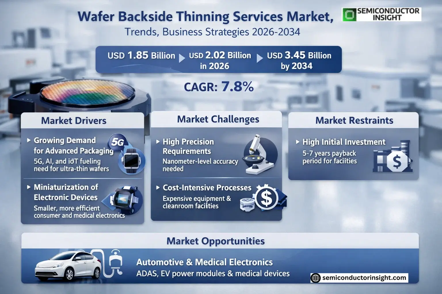
Global Wafer Backside Thinning Services Market size was valued at USD 1.85 billion in 2025. The market is projected to grow from USD 2.02 billion in 2026 to USD 3.45 billion by 2034, exhibiting a CAGR of 7.8% during the forecast period.

Wafer backside thinning services involve precision processes such as grinding and etching to reduce the thickness of semiconductor wafers, enhancing performance and enabling advanced packaging solutions. These services are critical for applications in consumer electronics, automotive electronics, and data centers, where thinner wafers improve thermal management and device integration.

The market is driven by increasing demand for compact and high-performance semiconductor devices, alongside advancements in wafer-level packaging technologies. Key players like DISCO Corporation and Silicon Valley Microelectronics are expanding their capabilities to meet rising industry requirements, further accelerating market growth.

Wafer Backside Thinning Services Market Share

MARKET DRIVERS

Growing Demand for Advanced Semiconductor Packaging

Wafer Backside Thinning Services Market is experiencing significant growth due to the rising demand for advanced semiconductor packaging solutions. As consumer electronics and IoT devices become more compact, manufacturers require ultra-thin wafers to enable higher-density chip integration. Global shift toward 5G technology and AI applications has further accelerated this demand.

Miniaturization of Electronic Devices

With smartphones, wearables, and medical devices requiring increasingly smaller form factors, wafer backside thinning services have become essential. Thin wafers (below 100µm) allow for improved thermal performance and reduced power consumption in compact electronic components. Leading semiconductor foundries are investing heavily in wafer thinning technologies to meet these specifications.

Advanced wafer thinning techniques such as plasma etching and chemical-mechanical polishing are enabling manufacturers to achieve thicknesses below 50µm while maintaining structural integrity.

MARKET CHALLENGES

High Precision Requirements and Yield Management

The wafer backside thinning process requires nanometer-level precision to avoid cracks, warping, or contamination. Maintaining high yield rates while achieving ultra-thin profiles remains a critical challenge for service providers, as even minor defects can render wafers unusable for advanced applications.

Other Challenges

Cost-Intensive Equipment and Processes
Wafer backside thinning demands specialized equipment like grinders, polishers, and etching systems, which require significant capital investment. Additionally, the need for cleanroom facilities and skilled technicians adds to operational costs.

Thermal Management in Thin Wafers
As wafer thickness decreases below 70µm, managing heat dissipation becomes more complex, requiring additional engineering solutions that can increase production costs by 15-20%.

MARKET RESTRAINTS

High Initial Investment and Long Payback Periods

Wafer Backside Thinning Services Market faces limitations due to the substantial capital required for establishing production facilities. Smaller foundries often opt for outsourcing rather than developing in-house capabilities, which can slow market expansion. The average payback period for a wafer thinning production line currently ranges between 5-7 years.

MARKET OPPORTUNITIES

Emerging Applications in Automotive and Medical Electronics

Wafer Backside Thinning Services Market is witnessing new growth opportunities from the automotive sector, where thin wafers are critical for advanced driver assistance systems (ADAS) and electric vehicle power modules. Medical device manufacturers are also adopting wafer thinning for implantable electronics and miniature diagnostic equipment. The medical electronics segment is expected to grow at 8.2% annually through 2028.

Wafer Backside Thinning Services Market Trends
Rising Demand for Advanced Semiconductor Packaging

Wafer Backside Thinning Services Market is experiencing growth driven by increasing demand for advanced packaging solutions in semiconductor manufacturing. Thinning processes enable better thermal management and miniaturization, critical for modern electronics. Companies are adopting wafer thinning to meet performance requirements in applications like consumer electronics and automotive systems.

Other Trends

Expansion of Grinding Technology

Grinding remains the dominant wafer backside thinning method due to its precision and cost-effectiveness. Technological advancements in grinding equipment allow for ultra-thin wafers below 50μm thickness, meeting the needs of 3D IC packaging and MEMS applications. Manufacturers are investing in automated grinding solutions to enhance throughput.

Geographical Market Shifts

Asia-Pacific continues to lead in wafer backside thinning adoption, with China and Japan driving demand from foundries and IDMs. North America shows steady growth, particularly in high-performance computing applications. European markets are focusing on thin-wafer solutions for automotive and industrial electronics.

Emerging Applications Driving Innovation

The development of 5G infrastructure, IoT devices, and AI hardware is creating new opportunities for wafer thinning services. These applications require thinner, more efficient semiconductor components, pushing service providers to develop advanced thinning techniques with improved yield rates and surface quality.

Competitive Landscape Developments

Key players like DISCO Corporation and Syagrus Systems are expanding their service capabilities to include hybrid thinning approaches combining mechanical and chemical methods. The market is seeing increased specialization, with some providers focusing on niche applications such as photonics or power devices.

COMPETITIVE LANDSCAPE

Key Industry Players

Global Market Dominated by Specialized Semiconductor Service Providers

Wafer Backside Thinning Services Market is characterized by a concentrated competitive landscape, with leading players like DISCO Corporation and Syagrus Systems controlling significant market share through advanced grinding and etching technologies. These established providers maintain dominance through proprietary equipment, precision engineering capabilities, and strategic partnerships with major semiconductor fabs. The top five companies collectively accounted for approximately XX% of global revenue in 2025, with technological differentiation in ultra-thin wafer processing (sub-50μm) serving as a key competitive battleground.

Several specialized manufacturers have carved out strong positions in niche segments, including Silicon Valley Microelectronics for MEMS applications and NICHIWA KOGYO for compound semiconductor substrates. Emerging players such as Huahong Group and Winstek are gaining traction in Asian markets through cost-competitive service models, while technology-focused firms like Helia Photonics compete through innovative thinning solutions for photonic applications. Regional specialists like Phoenix Silicon International have strengthened their positions through localized service networks and quick turnaround capabilities.

List of Key Wafer Backside Thinning Services Companies Profiled

Segment Analysis:

Segment Category Sub-Segments Key Insights
By Type
  • Grinding
  • Etching
  • Others
Grinding dominates the market as the preferred wafer thinning technique due to:

  • Higher precision and control for advanced semiconductor packaging
  • Better surface finish quality compared to alternative methods
  • Wider adoption in high-volume manufacturing environments
By Application
  • Consumer Electronics
  • Automotive Electronics
  • Computer and Data Center
  • Others
Consumer Electronics represents the largest application segment because:

  • Increasing demand for thinner semiconductor packages in smartphones and wearables
  • Growing need for advanced packaging solutions in IoT devices
  • Continuous innovation in portable electronics requiring thinner wafers
By End User
  • IDMs (Integrated Device Manufacturers)
  • Foundries
  • OSATs (Outsourced Semiconductor Assembly and Test)
Foundries are the primary users of wafer thinning services due to:

  • Increasing adoption of wafer-level packaging in semiconductor manufacturing
  • Focus on offering complete manufacturing solutions to fabless companies
  • Strategic partnerships with specialty wafer service providers
By Wafer Size
  • 200mm
  • 300mm
  • Larger than 300mm
300mm wafers show strongest demand for backside thinning because:

  • Dominant position in advanced logic and memory manufacturing
  • Higher cost-effectiveness in high-volume production environments
  • Growing adoption in cutting-edge applications like 5G and AI chips
By Service Provider
  • Pure-play Thinning Specialists
  • Integrated Semiconductor Services
  • Captive Provider Services
Pure-play Thinning Specialists maintain leadership through:

  • Specialized technical expertise in wafer thinning processes
  • Investment in proprietary thinning technologies
  • Ability to serve diverse customer needs across multiple industries

Regional Analysis: Wafer Backside Thinning Services Market

Asia-Pacific

The Asia-Pacific region dominates the Wafer Backside Thinning Services Market, driven by its robust semiconductor manufacturing ecosystem and increasing demand for advanced packaging solutions. Countries like Taiwan, South Korea, and China are at the forefront, housing major foundries and OSAT players that require precision thinning services. The region benefits from strong government support for semiconductor self-sufficiency, with China’s national semiconductor fund and Taiwan’s specialized R&D initiatives fostering local capabilities. Leading manufacturers are investing heavily in 200mm and 300mm wafer thinning technologies to support 3D IC packaging trends. The proximity to end-use electronics manufacturers creates an efficient supply chain for wafer-level packaging services, with Japanese equipment manufacturers providing cutting-edge thinning solutions to local foundries.

Technology Leadership
Asia-Pacific leads in adopting advanced wafer backside thinning techniques like temporary bonding/debonding and ultra-thin wafer handling, with Taiwanese firms pioneering sub-50μm thinning capabilities for 3D IC applications.
Manufacturing Infrastructure
The region boasts the world’s highest concentration of 300mm wafer fabs, creating concentrated demand for high-volume backside thinning services near major semiconductor clusters in Hsinchu, Shanghai and Pyeongtaek.
Supply Chain Integration
Close collaboration between thinning service providers, equipment manufacturers and OSAT companies enables seamless integration from wafer fabrication to packaging, reducing logistics costs and cycle times.
Emerging Applications
Growing demand for wafer thinning services comes from advanced packaging applications including CIS, MEMS sensors and power devices, with Chinese manufacturers rapidly expanding capabilities for automotive and IoT chips.

North America
North America maintains leadership in specialized wafer backside thinning services for high-performance computing and aerospace applications. The region benefits from strong R&D capabilities and demand from fabless semiconductor companies that outsource advanced packaging needs. Major IDMs in the US are investing in wafer-level packaging solutions to support AI/ML processors requiring ultra-thin wafers. The presence of leading equipment manufacturers enables access to cutting-edge thinning technologies, though local thinning service capacity remains limited compared to Asia, leading to partnerships with overseas providers.

Europe
Europe’s wafer backside thinning market is characterized by specialized applications in automotive and industrial sectors, with Germany and France leading in MEMS and power device production. The region has developed niche expertise in handling compound semiconductor wafers for RF applications. While lacking Asia’s volume capacity, European service providers focus on high-mix, low-volume production with stringent quality requirements. Collaborative R&D projects under EU semiconductor initiatives are driving development of advanced thinning techniques for next-generation power electronics.

Middle East & Africa
The MEA region is emerging as a potential market for wafer backside thinning services, with growing semiconductor packaging activity in Israel and limited foundry operations in the UAE. Most regional demand is met through partnerships with global service providers, though local capabilities remain limited. The region shows potential for specialized applications in aerospace and defense sectors, with investments in compound semiconductor manufacturing creating future opportunities for localized thinning services.

South America
South America remains a minor player in wafer backside thinning services, with limited semiconductor manufacturing infrastructure. Brazil has some packaging and test operations that utilize basic thinning services, primarily sourced from international providers. The region’s market potential is constrained by limited local semiconductor production, though growing electronics manufacturing could drive future demand for basic backside thinning solutions.

Report Scope

This market research report provides a comprehensive analysis of the Wafer Backside Thinning Services Market , covering the forecast period 2025–2034. It offers detailed insights into market dynamics, technological advancements, competitive landscape, and key trends shaping the industry.

Key focus areas of the report include:

  • Market Overview: The report begins with an overview outlining its current market scenario, key growth indicators, and industry transformation drivers. It discusses macroeconomic factors, demand–supply balance, regulatory landscape, and the strategic role of wafer thinning in powering advancements across industries such as consumer electronics, automotive electronics, and data centers.
  • Market Size & Forecast: Historical data and future projections for revenue, unit shipments, and market value across major regions and segments.
  • Segmentation Analysis: Detailed breakdown by product type (Grinding, Etching, Others), technology, application, and end-user industry to identify high-growth segments and investment opportunities.
  • Regional Insights: Insights into market performance across North America, Europe, Asia, South America, and Middle East & Africa, including country-level analysis.
  • Competitive Landscape: Profiles of leading market participants, including their product offerings, R&D focus, manufacturing capacity, pricing strategies, and recent developments.
  • Technology Trends & Innovation: Assessment of emerging wafer thinning technologies, fabrication techniques, and evolving industry standards.
  • Market Drivers & Restraints: Evaluation of factors driving market growth along with challenges, supply chain constraints, and market-entry barriers.
  • Stakeholder Insights: Insights for wafer manufacturers, OEMs, system integrators, and investors regarding strategic opportunities.

Primary and secondary research methods are employed, including interviews with industry experts and data from verified sources to ensure accuracy and reliability.

FREQUENTLY ASKED QUESTIONS:

What is the current market size of Wafer Backside Thinning Services Market?

-> Wafer Backside Thinning Services Market size was valued at USD 1.85 billion in 2025. The market is projected to grow from USD 2.02 billion in 2026 to USD 3.45 billion by 2034, exhibiting a CAGR of 7.8% during the forecast period.

What is the growth rate (CAGR) of Wafer Backside Thinning Services Market?

-> The market is expected to grow at a CAGR of % during 2025-2034.

Which are the key players in Wafer Backside Thinning Services Market?

-> Key players include Syagrus Systems, Optim Wafer Services, Silicon Valley Microelectronics, SIEGERT WAFER GmbH, DISCO Corporation, AXUS TECHNOLOGY, and other leading companies.

Which segment leads the market by product type?

-> Grinding segment dominates the market and is projected to reach USD million by 2034.

Which region shows highest growth potential?

-> China is expected to reach USD million by 2034, showing significant growth potential.

What are the main applications of Wafer Backside Thinning Services?

-> Key applications include Consumer Electronics, Automotive Electronics, and Computer and Data Center sectors.

Wafer Backside Thinning Services Market, Trends, Business Strategies 2026-2034

Get Sample Report PDF for Exclusive Insights

Report Sample Includes

  • Table of Contents
  • List of Tables & Figures
  • Charts, Research Methodology, and more...
PDF Icon Download Sample Report PDF
SKU: c3cc727e463a
Category:
License Type

Corporate License, Excel License, PDF and Excel Databook License

Download Sample Report

Table of Content

1 Introduction to Research & Analysis Reports
1.1 Wafer Backside Thinning Services Market Definition
1.2 Market Segments
1.2.1 Segment by Type
1.2.2 Segment by Application
1.3 Global Wafer Backside Thinning Services Market Overview
1.4 Features & Benefits of This Report
1.5 Methodology & Sources of Information
1.5.1 Research Methodology
1.5.2 Research Process
1.5.3 Base Year
1.5.4 Report Assumptions & Caveats
2 Global Wafer Backside Thinning Services Overall Market Size
2.1 Global Wafer Backside Thinning Services Market Size: 2025 VS 2034
2.2 Global Wafer Backside Thinning Services Market Size, Prospects & Forecasts: 2021-2034
2.3 Key Market Trends, Opportunity, Drivers and Restraints
2.3.1 Market Opportunities & Trends
2.3.2 Market Drivers
2.3.3 Market Restraints
3 Company Landscape
3.1 Top Wafer Backside Thinning Services Players in Global Market
3.2 Top Global Wafer Backside Thinning Services Companies Ranked by Revenue
3.3 Global Wafer Backside Thinning Services Revenue by Companies
3.4 Top 3 and Top 5 Wafer Backside Thinning Services Companies in Global Market, by Revenue in 2025
3.5 Global Companies Wafer Backside Thinning Services Product Type
3.6 Tier 1, Tier 2, and Tier 3 Wafer Backside Thinning Services Players in Global Market
3.6.1 List of Global Tier 1 Wafer Backside Thinning Services Companies
3.6.2 List of Global Tier 2 and Tier 3 Wafer Backside Thinning Services Companies
4 Sights by Type
4.1 Overview
4.1.1 Segmentation by Type – Global Wafer Backside Thinning Services Market Size Markets, 2025 & 2034
4.1.2 Grinding
4.1.3 Etching
4.1.4 Others
4.2 Segmentation by Type – Global Wafer Backside Thinning Services Revenue & Forecasts
4.2.1 Segmentation by Type – Global Wafer Backside Thinning Services Revenue, 2021-2026
4.2.2 Segmentation by Type – Global Wafer Backside Thinning Services Revenue, 2027-2034
4.2.3 Segmentation by Type – Global Wafer Backside Thinning Services Revenue Market Share, 2021-2034
5 Sights by Application
5.1 Overview
5.1.1 Segmentation by Application – Global Wafer Backside Thinning Services Market Size, 2025 & 2034
5.1.2 Consumer Electronics
5.1.3 Automotive Electronics
5.1.4 Computer and Data Center
5.1.5 Others
5.2 Segmentation by Application – Global Wafer Backside Thinning Services Revenue & Forecasts
5.2.1 Segmentation by Application – Global Wafer Backside Thinning Services Revenue, 2021-2026
5.2.2 Segmentation by Application – Global Wafer Backside Thinning Services Revenue, 2027-2034
5.2.3 Segmentation by Application – Global Wafer Backside Thinning Services Revenue Market Share, 2021-2034
6 Sights Region
6.1 By Region – Global Wafer Backside Thinning Services Market Size, 2025 & 2034
6.2 By Region – Global Wafer Backside Thinning Services Revenue & Forecasts
6.2.1 By Region – Global Wafer Backside Thinning Services Revenue, 2021-2026
6.2.2 By Region – Global Wafer Backside Thinning Services Revenue, 2027-2034
6.2.3 By Region – Global Wafer Backside Thinning Services Revenue Market Share, 2021-2034
6.3 North America
6.3.1 By Country – North America Wafer Backside Thinning Services Revenue, 2021-2034
6.3.2 United States Wafer Backside Thinning Services Market Size, 2021-2034
6.3.3 Canada Wafer Backside Thinning Services Market Size, 2021-2034
6.3.4 Mexico Wafer Backside Thinning Services Market Size, 2021-2034
6.4 Europe
6.4.1 By Country – Europe Wafer Backside Thinning Services Revenue, 2021-2034
6.4.2 Germany Wafer Backside Thinning Services Market Size, 2021-2034
6.4.3 France Wafer Backside Thinning Services Market Size, 2021-2034
6.4.4 U.K. Wafer Backside Thinning Services Market Size, 2021-2034
6.4.5 Italy Wafer Backside Thinning Services Market Size, 2021-2034
6.4.6 Russia Wafer Backside Thinning Services Market Size, 2021-2034
6.4.7 Nordic Countries Wafer Backside Thinning Services Market Size, 2021-2034
6.4.8 Benelux Wafer Backside Thinning Services Market Size, 2021-2034
6.5 Asia
6.5.1 By Region – Asia Wafer Backside Thinning Services Revenue, 2021-2034
6.5.2 China Wafer Backside Thinning Services Market Size, 2021-2034
6.5.3 Japan Wafer Backside Thinning Services Market Size, 2021-2034
6.5.4 South Korea Wafer Backside Thinning Services Market Size, 2021-2034
6.5.5 Southeast Asia Wafer Backside Thinning Services Market Size, 2021-2034
6.5.6 India Wafer Backside Thinning Services Market Size, 2021-2034
6.6 South America
6.6.1 By Country – South America Wafer Backside Thinning Services Revenue, 2021-2034
6.6.2 Brazil Wafer Backside Thinning Services Market Size, 2021-2034
6.6.3 Argentina Wafer Backside Thinning Services Market Size, 2021-2034
6.7 Middle East & Africa
6.7.1 By Country – Middle East & Africa Wafer Backside Thinning Services Revenue, 2021-2034
6.7.2 Turkey Wafer Backside Thinning Services Market Size, 2021-2034
6.7.3 Israel Wafer Backside Thinning Services Market Size, 2021-2034
6.7.4 Saudi Arabia Wafer Backside Thinning Services Market Size, 2021-2034
6.7.5 UAE Wafer Backside Thinning Services Market Size, 2021-2034
7 Companies Profiles
7.1 Syagrus Systems
7.1.1 Syagrus Systems Corporate Summary
7.1.2 Syagrus Systems Business Overview
7.1.3 Syagrus Systems Wafer Backside Thinning Services Major Product Offerings
7.1.4 Syagrus Systems Wafer Backside Thinning Services Revenue in Global Market (2021-2026)
7.1.5 Syagrus Systems Key News & Latest Developments
7.2 Optim Wafer Services
7.2.1 Optim Wafer Services Corporate Summary
7.2.2 Optim Wafer Services Business Overview
7.2.3 Optim Wafer Services Wafer Backside Thinning Services Major Product Offerings
7.2.4 Optim Wafer Services Wafer Backside Thinning Services Revenue in Global Market (2021-2026)
7.2.5 Optim Wafer Services Key News & Latest Developments
7.3 Silicon Valley Microelectronics, Inc.
7.3.1 Silicon Valley Microelectronics, Inc. Corporate Summary
7.3.2 Silicon Valley Microelectronics, Inc. Business Overview
7.3.3 Silicon Valley Microelectronics, Inc. Wafer Backside Thinning Services Major Product Offerings
7.3.4 Silicon Valley Microelectronics, Inc. Wafer Backside Thinning Services Revenue in Global Market (2021-2026)
7.3.5 Silicon Valley Microelectronics, Inc. Key News & Latest Developments
7.4 SIEGERT WAFER GmbH
7.4.1 SIEGERT WAFER GmbH Corporate Summary
7.4.2 SIEGERT WAFER GmbH Business Overview
7.4.3 SIEGERT WAFER GmbH Wafer Backside Thinning Services Major Product Offerings
7.4.4 SIEGERT WAFER GmbH Wafer Backside Thinning Services Revenue in Global Market (2021-2026)
7.4.5 SIEGERT WAFER GmbH Key News & Latest Developments
7.5 NICHIWA KOGYO CO.,LTD.
7.5.1 NICHIWA KOGYO CO.,LTD. Corporate Summary
7.5.2 NICHIWA KOGYO CO.,LTD. Business Overview
7.5.3 NICHIWA KOGYO CO.,LTD. Wafer Backside Thinning Services Major Product Offerings
7.5.4 NICHIWA KOGYO CO.,LTD. Wafer Backside Thinning Services Revenue in Global Market (2021-2026)
7.5.5 NICHIWA KOGYO CO.,LTD. Key News & Latest Developments
7.6 Integra Technologies
7.6.1 Integra Technologies Corporate Summary
7.6.2 Integra Technologies Business Overview
7.6.3 Integra Technologies Wafer Backside Thinning Services Major Product Offerings
7.6.4 Integra Technologies Wafer Backside Thinning Services Revenue in Global Market (2021-2026)
7.6.5 Integra Technologies Key News & Latest Developments
7.7 Valley Design
7.7.1 Valley Design Corporate Summary
7.7.2 Valley Design Business Overview
7.7.3 Valley Design Wafer Backside Thinning Services Major Product Offerings
7.7.4 Valley Design Wafer Backside Thinning Services Revenue in Global Market (2021-2026)
7.7.5 Valley Design Key News & Latest Developments
7.8 AXUS TECHNOLOGY
7.8.1 AXUS TECHNOLOGY Corporate Summary
7.8.2 AXUS TECHNOLOGY Business Overview
7.8.3 AXUS TECHNOLOGY Wafer Backside Thinning Services Major Product Offerings
7.8.4 AXUS TECHNOLOGY Wafer Backside Thinning Services Revenue in Global Market (2021-2026)
7.8.5 AXUS TECHNOLOGY Key News & Latest Developments
7.9 Helia Photonics
7.9.1 Helia Photonics Corporate Summary
7.9.2 Helia Photonics Business Overview
7.9.3 Helia Photonics Wafer Backside Thinning Services Major Product Offerings
7.9.4 Helia Photonics Wafer Backside Thinning Services Revenue in Global Market (2021-2026)
7.9.5 Helia Photonics Key News & Latest Developments
7.10 DISCO Corporation
7.10.1 DISCO Corporation Corporate Summary
7.10.2 DISCO Corporation Business Overview
7.10.3 DISCO Corporation Wafer Backside Thinning Services Major Product Offerings
7.10.4 DISCO Corporation Wafer Backside Thinning Services Revenue in Global Market (2021-2026)
7.10.5 DISCO Corporation Key News & Latest Developments
7.11 Aptek Industries
7.11.1 Aptek Industries Corporate Summary
7.11.2 Aptek Industries Business Overview
7.11.3 Aptek Industries Wafer Backside Thinning Services Major Product Offerings
7.11.4 Aptek Industries Wafer Backside Thinning Services Revenue in Global Market (2021-2026)
7.11.5 Aptek Industries Key News & Latest Developments
7.12 UniversityWafer, Inc.
7.12.1 UniversityWafer, Inc. Corporate Summary
7.12.2 UniversityWafer, Inc. Business Overview
7.12.3 UniversityWafer, Inc. Wafer Backside Thinning Services Major Product Offerings
7.12.4 UniversityWafer, Inc. Wafer Backside Thinning Services Revenue in Global Market (2021-2026)
7.12.5 UniversityWafer, Inc. Key News & Latest Developments
7.13 Enzan Factory Co., Ltd.
7.13.1 Enzan Factory Co., Ltd. Corporate Summary
7.13.2 Enzan Factory Co., Ltd. Business Overview
7.13.3 Enzan Factory Co., Ltd. Wafer Backside Thinning Services Major Product Offerings
7.13.4 Enzan Factory Co., Ltd. Wafer Backside Thinning Services Revenue in Global Market (2021-2026)
7.13.5 Enzan Factory Co., Ltd. Key News & Latest Developments
7.14 Phoenix Silicon International
7.14.1 Phoenix Silicon International Corporate Summary
7.14.2 Phoenix Silicon International Business Overview
7.14.3 Phoenix Silicon International Wafer Backside Thinning Services Major Product Offerings
7.14.4 Phoenix Silicon International Wafer Backside Thinning Services Revenue in Global Market (2021-2026)
7.14.5 Phoenix Silicon International Key News & Latest Developments
7.15 Prosperity Power Technology Inc.
7.15.1 Prosperity Power Technology Inc. Corporate Summary
7.15.2 Prosperity Power Technology Inc. Business Overview
7.15.3 Prosperity Power Technology Inc. Wafer Backside Thinning Services Major Product Offerings
7.15.4 Prosperity Power Technology Inc. Wafer Backside Thinning Services Revenue in Global Market (2021-2026)
7.15.5 Prosperity Power Technology Inc. Key News & Latest Developments
7.16 Huahong Group
7.16.1 Huahong Group Corporate Summary
7.16.2 Huahong Group Business Overview
7.16.3 Huahong Group Wafer Backside Thinning Services Major Product Offerings
7.16.4 Huahong Group Wafer Backside Thinning Services Revenue in Global Market (2021-2026)
7.16.5 Huahong Group Key News & Latest Developments
7.17 MACMIC
7.17.1 MACMIC Corporate Summary
7.17.2 MACMIC Business Overview
7.17.3 MACMIC Wafer Backside Thinning Services Major Product Offerings
7.17.4 MACMIC Wafer Backside Thinning Services Revenue in Global Market (2021-2026)
7.17.5 MACMIC Key News & Latest Developments
7.18 Winstek
7.18.1 Winstek Corporate Summary
7.18.2 Winstek Business Overview
7.18.3 Winstek Wafer Backside Thinning Services Major Product Offerings
7.18.4 Winstek Wafer Backside Thinning Services Revenue in Global Market (2021-2026)
7.18.5 Winstek Key News & Latest Developments
8 Conclusion
9 Appendix
9.1 Note
9.2 Examples of Clients
9.3 DisclaimerList of Tables
Table 1. Wafer Backside Thinning Services Market Opportunities & Trends in Global Market
Table 2. Wafer Backside Thinning Services Market Drivers in Global Market
Table 3. Wafer Backside Thinning Services Market Restraints in Global Market
Table 4. Key Players of Wafer Backside Thinning Services in Global Market
Table 5. Top Wafer Backside Thinning Services Players in Global Market, Ranking by Revenue (2025)
Table 6. Global Wafer Backside Thinning Services Revenue by Companies, (US$, Mn), 2021-2026
Table 7. Global Wafer Backside Thinning Services Revenue Share by Companies, 2021-2026
Table 8. Global Companies Wafer Backside Thinning Services Product Type
Table 9. List of Global Tier 1 Wafer Backside Thinning Services Companies, Revenue (US$, Mn) in 2025 and Market Share
Table 10. List of Global Tier 2 and Tier 3 Wafer Backside Thinning Services Companies, Revenue (US$, Mn) in 2025 and Market Share
Table 11. Segmentation by Type – Global Wafer Backside Thinning Services Revenue, (US$, Mn), 2025 & 2034
Table 12. Segmentation by Type – Global Wafer Backside Thinning Services Revenue (US$, Mn), 2021-2026
Table 13. Segmentation by Type – Global Wafer Backside Thinning Services Revenue (US$, Mn), 2027-2034
Table 14. Segmentation by Application– Global Wafer Backside Thinning Services Revenue, (US$, Mn), 2025 & 2034
Table 15. Segmentation by Application – Global Wafer Backside Thinning Services Revenue, (US$, Mn), 2021-2026
Table 16. Segmentation by Application – Global Wafer Backside Thinning Services Revenue, (US$, Mn), 2027-2034
Table 17. By Region– Global Wafer Backside Thinning Services Revenue, (US$, Mn), 2025 & 2034
Table 18. By Region – Global Wafer Backside Thinning Services Revenue, (US$, Mn), 2021-2026
Table 19. By Region – Global Wafer Backside Thinning Services Revenue, (US$, Mn), 2027-2034
Table 20. By Country – North America Wafer Backside Thinning Services Revenue, (US$, Mn), 2021-2026
Table 21. By Country – North America Wafer Backside Thinning Services Revenue, (US$, Mn), 2027-2034
Table 22. By Country – Europe Wafer Backside Thinning Services Revenue, (US$, Mn), 2021-2026
Table 23. By Country – Europe Wafer Backside Thinning Services Revenue, (US$, Mn), 2027-2034
Table 24. By Region – Asia Wafer Backside Thinning Services Revenue, (US$, Mn), 2021-2026
Table 25. By Region – Asia Wafer Backside Thinning Services Revenue, (US$, Mn), 2027-2034
Table 26. By Country – South America Wafer Backside Thinning Services Revenue, (US$, Mn), 2021-2026
Table 27. By Country – South America Wafer Backside Thinning Services Revenue, (US$, Mn), 2027-2034
Table 28. By Country – Middle East & Africa Wafer Backside Thinning Services Revenue, (US$, Mn), 2021-2026
Table 29. By Country – Middle East & Africa Wafer Backside Thinning Services Revenue, (US$, Mn), 2027-2034
Table 30. Syagrus Systems Corporate Summary
Table 31. Syagrus Systems Wafer Backside Thinning Services Product Offerings
Table 32. Syagrus Systems Wafer Backside Thinning Services Revenue (US$, Mn) & (2021-2026)
Table 33. Syagrus Systems Key News & Latest Developments
Table 34. Optim Wafer Services Corporate Summary
Table 35. Optim Wafer Services Wafer Backside Thinning Services Product Offerings
Table 36. Optim Wafer Services Wafer Backside Thinning Services Revenue (US$, Mn) & (2021-2026)
Table 37. Optim Wafer Services Key News & Latest Developments
Table 38. Silicon Valley Microelectronics, Inc. Corporate Summary
Table 39. Silicon Valley Microelectronics, Inc. Wafer Backside Thinning Services Product Offerings
Table 40. Silicon Valley Microelectronics, Inc. Wafer Backside Thinning Services Revenue (US$, Mn) & (2021-2026)
Table 41. Silicon Valley Microelectronics, Inc. Key News & Latest Developments
Table 42. SIEGERT WAFER GmbH Corporate Summary
Table 43. SIEGERT WAFER GmbH Wafer Backside Thinning Services Product Offerings
Table 44. SIEGERT WAFER GmbH Wafer Backside Thinning Services Revenue (US$, Mn) & (2021-2026)
Table 45. SIEGERT WAFER GmbH Key News & Latest Developments
Table 46. NICHIWA KOGYO CO.,LTD. Corporate Summary
Table 47. NICHIWA KOGYO CO.,LTD. Wafer Backside Thinning Services Product Offerings
Table 48. NICHIWA KOGYO CO.,LTD. Wafer Backside Thinning Services Revenue (US$, Mn) & (2021-2026)
Table 49. NICHIWA KOGYO CO.,LTD. Key News & Latest Developments
Table 50. Integra Technologies Corporate Summary
Table 51. Integra Technologies Wafer Backside Thinning Services Product Offerings
Table 52. Integra Technologies Wafer Backside Thinning Services Revenue (US$, Mn) & (2021-2026)
Table 53. Integra Technologies Key News & Latest Developments
Table 54. Valley Design Corporate Summary
Table 55. Valley Design Wafer Backside Thinning Services Product Offerings
Table 56. Valley Design Wafer Backside Thinning Services Revenue (US$, Mn) & (2021-2026)
Table 57. Valley Design Key News & Latest Developments
Table 58. AXUS TECHNOLOGY Corporate Summary
Table 59. AXUS TECHNOLOGY Wafer Backside Thinning Services Product Offerings
Table 60. AXUS TECHNOLOGY Wafer Backside Thinning Services Revenue (US$, Mn) & (2021-2026)
Table 61. AXUS TECHNOLOGY Key News & Latest Developments
Table 62. Helia Photonics Corporate Summary
Table 63. Helia Photonics Wafer Backside Thinning Services Product Offerings
Table 64. Helia Photonics Wafer Backside Thinning Services Revenue (US$, Mn) & (2021-2026)
Table 65. Helia Photonics Key News & Latest Developments
Table 66. DISCO Corporation Corporate Summary
Table 67. DISCO Corporation Wafer Backside Thinning Services Product Offerings
Table 68. DISCO Corporation Wafer Backside Thinning Services Revenue (US$, Mn) & (2021-2026)
Table 69. DISCO Corporation Key News & Latest Developments
Table 70. Aptek Industries Corporate Summary
Table 71. Aptek Industries Wafer Backside Thinning Services Product Offerings
Table 72. Aptek Industries Wafer Backside Thinning Services Revenue (US$, Mn) & (2021-2026)
Table 73. Aptek Industries Key News & Latest Developments
Table 74. UniversityWafer, Inc. Corporate Summary
Table 75. UniversityWafer, Inc. Wafer Backside Thinning Services Product Offerings
Table 76. UniversityWafer, Inc. Wafer Backside Thinning Services Revenue (US$, Mn) & (2021-2026)
Table 77. UniversityWafer, Inc. Key News & Latest Developments
Table 78. Enzan Factory Co., Ltd. Corporate Summary
Table 79. Enzan Factory Co., Ltd. Wafer Backside Thinning Services Product Offerings
Table 80. Enzan Factory Co., Ltd. Wafer Backside Thinning Services Revenue (US$, Mn) & (2021-2026)
Table 81. Enzan Factory Co., Ltd. Key News & Latest Developments
Table 82. Phoenix Silicon International Corporate Summary
Table 83. Phoenix Silicon International Wafer Backside Thinning Services Product Offerings
Table 84. Phoenix Silicon International Wafer Backside Thinning Services Revenue (US$, Mn) & (2021-2026)
Table 85. Phoenix Silicon International Key News & Latest Developments
Table 86. Prosperity Power Technology Inc. Corporate Summary
Table 87. Prosperity Power Technology Inc. Wafer Backside Thinning Services Product Offerings
Table 88. Prosperity Power Technology Inc. Wafer Backside Thinning Services Revenue (US$, Mn) & (2021-2026)
Table 89. Prosperity Power Technology Inc. Key News & Latest Developments
Table 90. Huahong Group Corporate Summary
Table 91. Huahong Group Wafer Backside Thinning Services Product Offerings
Table 92. Huahong Group Wafer Backside Thinning Services Revenue (US$, Mn) & (2021-2026)
Table 93. Huahong Group Key News & Latest Developments
Table 94. MACMIC Corporate Summary
Table 95. MACMIC Wafer Backside Thinning Services Product Offerings
Table 96. MACMIC Wafer Backside Thinning Services Revenue (US$, Mn) & (2021-2026)
Table 97. MACMIC Key News & Latest Developments
Table 98. Winstek Corporate Summary
Table 99. Winstek Wafer Backside Thinning Services Product Offerings
Table 100. Winstek Wafer Backside Thinning Services Revenue (US$, Mn) & (2021-2026)
Table 101. Winstek Key News & Latest Developments

List of Figures
Figure 1. Wafer Backside Thinning Services Product Picture
Figure 2. Wafer Backside Thinning Services Segment by Type in 2025
Figure 3. Wafer Backside Thinning Services Segment by Application in 2025
Figure 4. Global Wafer Backside Thinning Services Market Overview: 2025
Figure 5. Key Caveats
Figure 6. Global Wafer Backside Thinning Services Market Size: 2025 VS 2034 (US$, Mn)
Figure 7. Global Wafer Backside Thinning Services Revenue: 2021-2034 (US$, Mn)
Figure 8. The Top 3 and 5 Players Market Share by Wafer Backside Thinning Services Revenue in 2025
Figure 9. Segmentation by Type – Global Wafer Backside Thinning Services Revenue, (US$, Mn), 2025 & 2034
Figure 10. Segmentation by Type – Global Wafer Backside Thinning Services Revenue Market Share, 2021-2034
Figure 11. Segmentation by Application – Global Wafer Backside Thinning Services Revenue, (US$, Mn), 2025 & 2034
Figure 12. Segmentation by Application – Global Wafer Backside Thinning Services Revenue Market Share, 2021-2034
Figure 13. By Region – Global Wafer Backside Thinning Services Revenue Market Share, 2021-2034
Figure 14. By Country – North America Wafer Backside Thinning Services Revenue Market Share, 2021-2034
Figure 15. United States Wafer Backside Thinning Services Revenue, (US$, Mn), 2021-2034
Figure 16. Canada Wafer Backside Thinning Services Revenue, (US$, Mn), 2021-2034
Figure 17. Mexico Wafer Backside Thinning Services Revenue, (US$, Mn), 2021-2034
Figure 18. By Country – Europe Wafer Backside Thinning Services Revenue Market Share, 2021-2034
Figure 19. Germany Wafer Backside Thinning Services Revenue, (US$, Mn), 2021-2034
Figure 20. France Wafer Backside Thinning Services Revenue, (US$, Mn), 2021-2034
Figure 21. U.K. Wafer Backside Thinning Services Revenue, (US$, Mn), 2021-2034
Figure 22. Italy Wafer Backside Thinning Services Revenue, (US$, Mn), 2021-2034
Figure 23. Russia Wafer Backside Thinning Services Revenue, (US$, Mn), 2021-2034
Figure 24. Nordic Countries Wafer Backside Thinning Services Revenue, (US$, Mn), 2021-2034
Figure 25. Benelux Wafer Backside Thinning Services Revenue, (US$, Mn), 2021-2034
Figure 26. By Region – Asia Wafer Backside Thinning Services Revenue Market Share, 2021-2034
Figure 27. China Wafer Backside Thinning Services Revenue, (US$, Mn), 2021-2034
Figure 28. Japan Wafer Backside Thinning Services Revenue, (US$, Mn), 2021-2034
Figure 29. South Korea Wafer Backside Thinning Services Revenue, (US$, Mn), 2021-2034
Figure 30. Southeast Asia Wafer Backside Thinning Services Revenue, (US$, Mn), 2021-2034
Figure 31. India Wafer Backside Thinning Services Revenue, (US$, Mn), 2021-2034
Figure 32. By Country – South America Wafer Backside Thinning Services Revenue Market Share, 2021-2034
Figure 33. Brazil Wafer Backside Thinning Services Revenue, (US$, Mn), 2021-2034
Figure 34. Argentina Wafer Backside Thinning Services Revenue, (US$, Mn), 2021-2034
Figure 35. By Country – Middle East & Africa Wafer Backside Thinning Services Revenue Market Share, 2021-2034
Figure 36. Turkey Wafer Backside Thinning Services Revenue, (US$, Mn), 2021-2034
Figure 37. Israel Wafer Backside Thinning Services Revenue, (US$, Mn), 2021-2034
Figure 38. Saudi Arabia Wafer Backside Thinning Services Revenue, (US$, Mn), 2021-2034
Figure 39. UAE Wafer Backside Thinning Services Revenue, (US$, Mn), 2021-2034
Figure 40. Syagrus Systems Wafer Backside Thinning Services Revenue Year Over Year Growth (US$, Mn) & (2021-2026)
Figure 41. Optim Wafer Services Wafer Backside Thinning Services Revenue Year Over Year Growth (US$, Mn) & (2021-2026)
Figure 42. Silicon Valley Microelectronics, Inc. Wafer Backside Thinning Services Revenue Year Over Year Growth (US$, Mn) & (2021-2026)
Figure 43. SIEGERT WAFER GmbH Wafer Backside Thinning Services Revenue Year Over Year Growth (US$, Mn) & (2021-2026)
Figure 44. NICHIWA KOGYO CO.,LTD. Wafer Backside Thinning Services Revenue Year Over Year Growth (US$, Mn) & (2021-2026)
Figure 45. Integra Technologies Wafer Backside Thinning Services Revenue Year Over Year Growth (US$, Mn) & (2021-2026)
Figure 46. Valley Design Wafer Backside Thinning Services Revenue Year Over Year Growth (US$, Mn) & (2021-2026)
Figure 47. AXUS TECHNOLOGY Wafer Backside Thinning Services Revenue Year Over Year Growth (US$, Mn) & (2021-2026)
Figure 48. Helia Photonics Wafer Backside Thinning Services Revenue Year Over Year Growth (US$, Mn) & (2021-2026)
Figure 49. DISCO Corporation Wafer Backside Thinning Services Revenue Year Over Year Growth (US$, Mn) & (2021-2026)
Figure 50. Aptek Industries Wafer Backside Thinning Services Revenue Year Over Year Growth (US$, Mn) & (2021-2026)
Figure 51. UniversityWafer, Inc. Wafer Backside Thinning Services Revenue Year Over Year Growth (US$, Mn) & (2021-2026)
Figure 52. Enzan Factory Co., Ltd. Wafer Backside Thinning Services Revenue Year Over Year Growth (US$, Mn) & (2021-2026)
Figure 53. Phoenix Silicon International Wafer Backside Thinning Services Revenue Year Over Year Growth (US$, Mn) & (2021-2026)
Figure 54. Prosperity Power Technology Inc. Wafer Backside Thinning Services Revenue Year Over Year Growth (US$, Mn) & (2021-2026)
Figure 55. Huahong Group Wafer Backside Thinning Services Revenue Year Over Year Growth (US$, Mn) & (2021-2026)
Figure 56. MACMIC Wafer Backside Thinning Services Revenue Year Over Year Growth (US$, Mn) & (2021-2026)
Figure 57. Winstek Wafer Backside Thinning Services Revenue Year Over Year Growth (US$, Mn) & (2021-2026)