Wafer Backside Grinding Service Market Insights
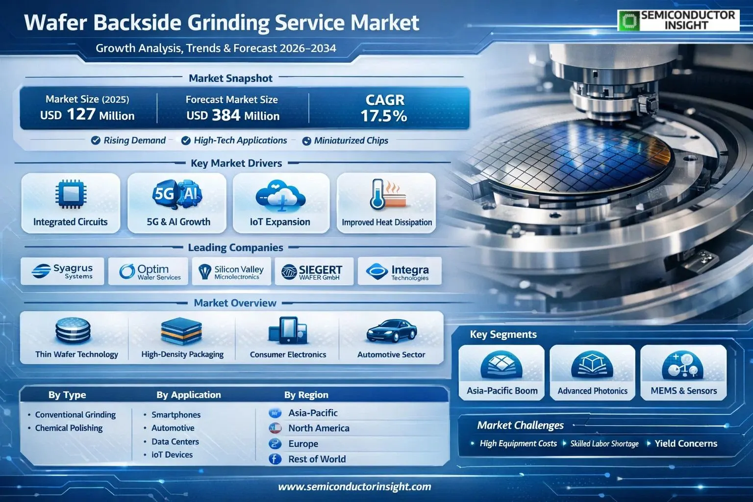
Global Wafer Backside Grinding Service market was valued at USD 127 million in 2025 and is projected to reach USD 384 million by 2034, exhibiting a CAGR of 17.5% during the forecast period.
Wafer backside grinding, also known as wafer thinning, is one of the semiconductor device manufacturing steps in which the wafer thickness is reduced to allow for the stacking and high-density packaging of integrated circuits (ICs). Integrated circuits are produced on semiconductor wafers that have undergone several processing steps. Silicon wafers commonly used today are around 750 micrometers thick to ensure maximum mechanical stability and avoid warping during high-temperature processing steps. Therefore, before wafer dicing, the back side of the wafer is ground or thinned. Today, wafers thinned to 75 to 50 micrometers are common.
The market is experiencing rapid growth due to surging demand from technologies such as integrated circuits, 5G, artificial intelligence, and the Internet of Things, especially in the Asia-Pacific region including China, South Korea, Japan, and Taiwan. These areas boast strong semiconductor manufacturing capabilities. Furthermore, rising needs in North America and Europe for high-performance computing are creating opportunities. Wafer thinning reduces chip size, improves heat dissipation, and boosts performance-to-power ratios. Despite challenges like high costs for advanced equipment, the outlook remains optimistic with maturing technology. Key players include Syagrus Systems, Optim Wafer Services, Silicon Valley Microelectronics, Inc., SIEGERT WAFER GmbH, NICHIWA KOGYO, and Integra Technologies.
MARKET DRIVERS
Rising Demand for Advanced Semiconductor Packaging
Wafer Backside Grinding Service Market is experiencing robust growth due to the increasing adoption of thin wafer technologies in high-performance computing and consumer electronics. Semiconductor manufacturers are pushing for wafer thicknesses below 50 microns to enable 3D stacking and heterogeneous integration, driving outsourcing to specialized service providers. This trend aligns with the global semiconductor market’s projected CAGR of 8.5% through 2028.
Expansion in 5G and AI Applications
Proliferation of 5G infrastructure and AI-driven devices necessitates ultra-thin wafers for improved thermal management and signal integrity, fueling demand for precise backside grinding services. Industry leaders report that over 70% of advanced nodes now require backside processing post-front-end fabrication. This shift underscores the market’s alignment with next-gen chiplet designs.
➤ Key players note a 25% year-over-year increase in service contracts for wafers under 100 microns, reflecting strong industry momentum.
Additionally, the rise in electric vehicle power modules, which demand thinned silicon carbide wafers, further accelerates Wafer Backside Grinding Service Market. With EV production expected to surpass 20 million units annually by 2025, service providers are scaling operations to meet this surge.
MARKET CHALLENGES
Technical Precision and Yield Optimization
Maintaining uniform thickness across large-diameter wafers, often 300mm or larger, poses significant hurdles in Wafer Backside Grinding Service Market. Variations as small as 1 micron can lead to warpage or cracking, impacting device reliability. Service providers invest heavily in temporary bonding and advanced polishing to mitigate these issues.
Other Challenges
Equipment and Skilled Labor Shortages
High-cost grinding tools and the need for certified technicians strain operations, with setup times extending project timelines. Approximately 40% of providers face delays due to supply chain disruptions for diamond wheels and slurries.
Competition from integrated device manufacturers developing in-house capabilities adds pressure, potentially eroding market share for third-party services. Despite these, the market’s growth trajectory remains positive as outsourcing benefits scale for smaller fabs.
MARKET RESTRAINTS
High Capital Intensity and Cost Barriers
Wafer Backside Grinding Service Market faces constraints from substantial upfront investments in cleanroom facilities and precision machinery, often exceeding $50 million per site. Smaller entrants struggle to compete, leading to market consolidation among top-tier providers.
Regulatory compliance for handling hazardous chemicals in grinding processes adds operational costs, particularly in regions with stringent environmental standards. This limits expansion in emerging markets where infrastructure lags.
Moreover, cyclical semiconductor demand fluctuations, such as those seen in 2023 downturns, restrain service utilization rates to around 75%, delaying ROI for new investments in Wafer Backside Grinding Service Market.
MARKET OPPORTUNITIES
Asia-Pacific Manufacturing Boom
Wafer Backside Grinding Service Market holds immense potential in Asia-Pacific, where over 60% of global semiconductor fabrication occurs. Rapid fab expansions in Taiwan, South Korea, and China create demand for outsourced thinning services amid capacity constraints.
Advancements in photonics and MEMS devices require specialized grinding for optical wafers, opening niches for service innovation. Projections indicate a 12% CAGR for these segments through 2030.
Strategic partnerships with OSAT firms for advanced packaging solutions position providers to capture growing volumes, especially as wafer sizes transition to 450mm. This evolution promises sustained expansion in Wafer Backside Grinding Service Market.
Wafer Backside Grinding Service Market Trends
Dominance of Asia-Pacific in Wafer Backside Grinding Services
The Asia-Pacific region, particularly China, South Korea, Japan, and Taiwan, leads Wafer Backside Grinding Service Market due to its robust semiconductor manufacturing infrastructure. These countries serve as primary production bases for semiconductors, driving substantial demand for wafer thinning processes essential for stacking and high-density packaging of integrated circuits. Wafer backside grinding reduces thickness from standard 750 micrometers to 50-75 micrometers, enabling compact devices like smartphones, smart cards, and USB memory sticks. This regional strength supports global supply chains, with ongoing investments in fabrication facilities amplifying service needs.
Other Trends
Technological Advancements from Emerging Applications
Developments in 5G, artificial intelligence, Internet of Things, and integrated circuits propel Wafer Backside Grinding Service Market forward. Wafer thinning enhances chip miniaturization, improves heat dissipation, and boosts performance-to-power ratios, critical for high-performance computing. Conventional grinding and chemical mechanical polishing (CMP) methods cater to diverse needs across consumer electronics, automotive electronics, computers, data centers, and other sectors. Despite challenges like larger wafer sizes requiring advanced equipment and higher maintenance costs, maturing technology expands applications and fosters service innovation.
Growth Opportunities in North America and Europe
In North America and Europe, rising demand stems from high-performance computing and artificial intelligence initiatives, creating new avenues for Wafer Backside Grinding Service Market expansion. Key players such as Syagrus Systems, Optim Wafer Services, Silicon Valley Microelectronics, and others are adapting to these shifts by refining processes for thinner wafers. Surveys of industry experts highlight trends toward diversified applications, addressing obstacles like technical complexities while capitalizing on drivers such as ultra-compact electronics proliferation. This balanced regional growth underscores the market’s resilience and potential for strategic service positioning amid evolving semiconductor demands.
COMPETITIVE LANDSCAPE
Key Industry Players
Leading Providers in the Global Wafer Backside Grinding Service Market
Wafer Backside Grinding Service Market exhibits a moderately fragmented competitive landscape, dominated by specialized providers offering precision thinning solutions essential for semiconductor manufacturing. Key leaders such as Syagrus Systems and Silicon Valley Microelectronics, Inc. command substantial market shares through advanced conventional grinding and chemical mechanical polishing (CMP) capabilities, catering to high-volume demands from consumer electronics and automotive sectors. Asia-Pacific firms, particularly from China, Japan, South Korea, and Taiwan, control over 70% of the global market due to proximity to major fabrication hubs and strong supply chains. This structure supports rapid innovation in wafer thinning to 50-75 micrometers, enabling stacking for 5G, AI, and IoT applications, with the market poised for 17.5% CAGR to US$384 million by 2034.
Complementing the frontrunners, niche players like SIEGERT WAFER GmbH, NICHIWA KOGYO, and Optim Wafer Services deliver customized services for ultra-thin wafers in high-performance computing and data centers. Emerging Asian competitors including Phoenix Silicon International, Huahong Group, and Winstek are gaining traction via investments in yield-enhancing technologies and regional expansions, while North American entities such as Integra Technologies focus on premium services for defense and aerospace. This diverse ecosystem fosters competition on throughput, defect rates, and cost-efficiency, with ongoing mergers and tech upgrades intensifying rivalry amid rising wafer sizes and integration complexities.
List of Key Wafer Backside Grinding Service Companies Profiled
- Syagrus Systems
- Optim Wafer Services
- Silicon Valley Microelectronics, Inc.
- SIEGERT WAFER GmbH
- NICHIWA KOGYO
- Integra Technologies
- Valley Design
- Helia Photonics
- Aptek Industries
- Enzan Factory Co., Ltd.
- Phoenix Silicon International
- Prosperity Power Technology Inc.
- Huahong Group
- Winstek
- CHIPBOND Technology Corporation
Segment Analysis:
| Segment Category | Sub-Segments | Key Insights |
| By Type |
|
Conventional Grinding remains the leading process in wafer backside grinding services.
|
| By Application |
|
Consumer Electronics drives the forefront of demand for backside grinding services.
|
| By End User |
|
Semiconductor Foundries represent the primary end users leveraging these services.
|
| By Wafer Size |
|
300 mm wafers dominate the service requirements.
|
| By Material Type |
|
Silicon leads as the foundational material for grinding services.
|
Regional Analysis: Wafer Backside Grinding Service Market
Asia-Pacific
Expansive investments in semiconductor foundries across Taiwan and South Korea amplify the need for reliable wafer backside grinding services. These facilities prioritize high-volume processing with tight tolerances to support advanced nodes, enabling service providers to specialize in temporary bonding and debonding workflows that preserve wafer integrity during thinning.
Japan and China’s R&D hubs pioneer stress-free grinding methods and dry polishing alternatives, reducing subsurface damage and enhancing die strength. This focus on next-generation techniques aligns with the push for 3D stacking and heterogeneous integration in Wafer Backside Grinding Service Market.
Robust local sourcing of abrasives and carrier wafers minimizes disruptions, allowing Asia-Pacific providers to maintain consistent service levels. Vertical integration trends strengthen partnerships between grinding specialists and chip assemblers, optimizing throughput for power semiconductors.
Rising adoption in electric vehicle power modules and 5G infrastructure propels service expansion. Providers adapt to diverse wafer materials, from silicon carbide to gallium nitride, meeting the nuanced requirements of high-voltage applications prevalent in the region.
North America
North America exhibits steady growth in Wafer Backside Grinding Service Market, fueled by innovation-centric ecosystems in the United States. Leading design houses and pilot fabs emphasize custom grinding solutions for leading-edge prototypes, particularly in AI accelerators and photonics. Service providers here excel in high-precision, low-volume processing with advanced metrology, supporting R&D for thinner wafers that enable stacked memory and sensors. Strategic partnerships with equipment vendors enhance capabilities in handling compound semiconductors. While manufacturing has partially shifted overseas, domestic incentives for onshoring critical processes bolster localized services. The focus remains on quality over scale, with providers differentiating through rapid turnaround and contamination-free environments tailored to defense and medical device sectors. This positions North America as a hub for bespoke grinding innovations amid global supply chain recalibrations.
Europe
Europe’s Wafer Backside Grinding Service Market thrives on specialized demand from automotive and industrial sectors, with Germany and the Netherlands at the core. Precision grinding services cater to silicon power devices for electric vehicles and renewable energy inverters, prioritizing mechanical stability and defect-free surfaces. Regional providers integrate grinding with edge trimming and coating steps, streamlining workflows for European chipmakers. Sustainability drives adoption of water-efficient processes and recyclable slurries, aligning with stringent environmental regulations. Collaborative consortia accelerate development of grinding for wide-bandgap materials, enhancing efficiency in power electronics. Though scale lags behind Asia-Pacific, Europe’s strength lies in high-value applications and quality certifications, fostering steady expansion through diversified end-markets like aerospace and smart grids.
South America
South America is an emerging player in Wafer Backside Grinding Service Market, with Brazil leading nascent efforts in semiconductor assembly and testing. Limited fab infrastructure directs focus toward outsourced grinding for consumer and automotive electronics, emphasizing cost-effective processes for standard silicon wafers. Local service providers build capabilities through technology transfers, targeting improvements in yield for mid-range devices. Regional growth hinges on expanding electronics manufacturing and government pushes for tech self-sufficiency. Challenges like infrastructure gaps are offset by partnerships with global firms, introducing automated grinding lines. As demand rises from agrotech sensors and telecom upgrades, South America positions itself for gradual integration into broader supply networks, leveraging proximity to key markets.
Middle East & Africa
The Middle East & Africa region shows potential in Wafer Backside Grinding Service Market, driven by diversification initiatives in the UAE and Israel. Israel’s advanced R&D in compound semiconductors spurs demand for specialized grinding in optoelectronics and defense applications, while Gulf states invest in fab facilities for regional chip production. Service providers adapt to harsh environments with robust equipment, focusing on high-reliability thinning for sensors and power management ICs. Emerging ecosystems benefit from international collaborations, enhancing skills in precision control and wafer handling. Growth is tempered by skill shortages but propelled by energy sector ties, particularly for silicon carbide devices in renewables. Strategic positioning as a logistics bridge between Asia and Europe further supports service maturation.
Report Scope
This market research report provides a comprehensive analysis of the Wafer Backside Grinding Service Market , covering the forecast period 2026–2034. It offers detailed insights into market dynamics, technological advancements, competitive landscape, and key trends shaping the industry.
Key focus areas of the report include:
- Market Overview: The report begins with an overview outlining its current market scenario, key growth indicators, and industry transformation drivers. It discusses macroeconomic factors, demand–supply balance, regulatory landscape, and the strategic role of semiconductors in powering advancements across industries such as automotive, telecommunications, consumer electronics, and industrial automation.
- Market Size & Forecast: Historical data and future projections for revenue, unit shipments, and market value across major regions and segments.
- Segmentation Analysis: Detailed breakdown by product type, technology, application, and end-user industry to identify high-growth segments and investment opportunities.
- Regional Insights: Insights into market performance across North America, Europe, Asia-Pacific, Latin America, and the Middle East & Africa, including country-level analysis where relevant.
- Competitive Landscape: Profiles of leading market participants, including their product offerings, R&D focus, manufacturing capacity, pricing strategies, and recent developments such as mergers, acquisitions, and partnerships.
- Technology Trends & Innovation: Assessment of emerging technologies, integration of AI/IoT, semiconductor design trends, fabrication techniques, and evolving industry standards.
- Market Drivers & Restraints: Evaluation of factors driving market growth along with challenges, supply chain constraints, regulatory issues, and market-entry barriers.
- Stakeholder Insights: Insights for component suppliers, OEMs, system integrators, investors, and policymakers regarding the evolving ecosystem and strategic opportunities.
Primary and secondary research methods are employed, including interviews with industry experts, data from verified sources, and real-time market intelligence to ensure the accuracy and reliability of the insights presented.
FREQUENTLY ASKED QUESTIONS:
What is the current market size of Wafer Backside Grinding Service Market?
-> Wafer Backside Grinding Service Market was valued at USD 127 million in 2025 and is expected to reach USD 384 million by 2034, at a CAGR of 17.5% during the forecast period.
Which key companies operate in Wafer Backside Grinding Service Market?
-> Key players include Syagrus Systems, Optim Wafer Services, Silicon Valley Microelectronics, Inc., SIEGERT WAFER GmbH, NICHIWA KOGYO, and Integra Technologies, among others.
What are the key growth drivers?
-> Key growth drivers include development of integrated circuits, 5G, artificial intelligence, Internet of Things, demand for miniaturized chips, improved heat dissipation, and high-performance computing.
Which region dominates the market?
-> Asia-Pacific is the main market, particularly China, South Korea, Japan, and Taiwan, with growth opportunities in North America and Europe from high-performance computing and AI.
What are the emerging trends?
-> Emerging trends include wafer thinning to 50-75 micrometers, high-density IC packaging, stacking technologies, and advancements in heat dissipation and performance-to-power ratio.

Get Sample Report PDF for Exclusive Insights
Report Sample Includes
- Table of Contents
- List of Tables & Figures
- Charts, Research Methodology, and more...
 Download Sample Report PDF