Market Insights
Global Third Generation Semiconductor Wafer Foundry Market size was valued at USD 316 million in 2025. The market is projected to grow from USD 387 million in 2026 to USD 1,271 million by 2034, exhibiting a CAGR of 22.5% during the forecast period.
Third generation semiconductor wafer foundries specialize in manufacturing silicon carbide (SiC) and gallium nitride (GaN) wafers, which offer superior performance in high-power, high-frequency, and high-temperature applications compared to traditional silicon-based semiconductors. These advanced materials enable critical innovations across industries such as electric vehicles, renewable energy systems, and 5G infrastructure.
The market growth is primarily driven by accelerating adoption of electric vehicles requiring efficient power electronics, expansion of 5G networks demanding high-frequency components, and increasing investments in energy-efficient power systems. While SiC wafer production remains concentrated among few specialized foundries like X-Fab and Episil Technology, GaN-on-Si wafer manufacturing has seen broader participation from major players including TSMC and GlobalFoundries. Recent capacity expansions by key manufacturers aim to address the growing demand-supply gap for these advanced semiconductor solutions.
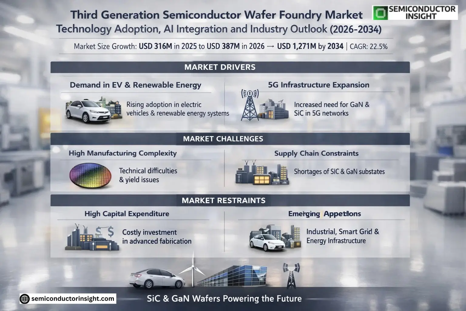
MARKET DRIVERS
Growing Demand for Power Electronics in EV and Renewable Energy
Third Generation Semiconductor Wafer Foundry Market is witnessing strong growth due to increasing adoption in electric vehicles and renewable energy systems. Wide bandgap materials like SiC and GaN enable higher efficiency power conversion, driving demand for specialized foundry services. Automotive manufacturers are rapidly transitioning to silicon carbide-based power modules to improve EV range and charging speeds.
5G Infrastructure Deployment Acceleration
Massive global 5G rollout is creating significant demand for gallium nitride wafers in RF power amplifiers. Third generation semiconductors offer superior high-frequency performance essential for 5G base stations, with foundries expanding capacity to meet telecom operator requirements. The market is projected to grow at 22% CAGR as 5G coverage expands worldwide.
Defense and aerospace applications are additionally driving specialized foundry requirements, particularly for radiation-hardened wide bandgap semiconductor solutions.
MARKET CHALLENGES
High Manufacturing Complexity and Yield Issues
Third Generation Semiconductor Wafer Foundry operations face significant technical challenges in maintaining production yields. The crystal growth and wafer processing of SiC and GaN materials require specialized equipment and process expertise, leading to higher defect rates compared to silicon wafers. Yield improvements are critical for cost-competitive mass production.
Other Challenges
Supply Chain Constraints for Raw Materials
Limited global capacity for high-purity silicon carbide and gallium nitride substrates creates bottlenecks in the Third Generation Semiconductor Wafer Foundry supply chain. Specialty gas suppliers are struggling to meet the rapid demand increase.
MARKET RESTRAINTS
High Capital Expenditure Requirements
Third Generation Semiconductor Wafer Foundry Market requires substantial investment in specialized fabrication equipment. New 200mm GaN and SiC production lines demand 2-3 times higher capital expenditure compared to equivalent silicon wafer fabs, creating barriers for new market entrants and limiting capacity expansion.
MARKET OPPORTUNITIES
Emerging Applications in Industrial and Energy Infrastructure
Third Generation Semiconductor Wafer Foundries are exploring significant growth potential in industrial motor drives and smart grid applications. The superior efficiency of SiC and GaN devices in high-voltage power conversion is creating new business opportunities in energy infrastructure modernization projects globally.
Third Generation Semiconductor Wafer Foundry Market Trends
Rising Demand for Advanced Power Electronics
Third Generation Semiconductor Wafer Foundry Market is experiencing significant growth driven by increasing adoption in power electronics applications. SiC and GaN wafers are crucial for high-voltage, high-temperature operations in electric vehicles, renewable energy systems, and industrial power converters. The automotive sector, particularly EV/HEV manufacturing, accounts for nearly 40% of wafer foundry demand as automakers transition to wide-bandgap semiconductors.
Other Trends
Technology Diversification in Foundry Services
Leading foundries are expanding capabilities for both SiC and GaN wafer production. While SiC dominates power electronics, GaN shows higher growth potential for RF applications in 5G infrastructure. Specialized foundries like X-Fab and Episil Technology are developing hybrid platforms to serve multiple technology segments.
Geographical Expansion of Manufacturing Capacity
Asia-Pacific remains the dominant region for Third Generation Semiconductor Wafer Foundry operations, with Taiwan, China, and South Korea housing major production facilities. However, North America and Europe are accelerating domestic capacity through government initiatives, aiming to reduce dependence on Asian supply chains. The U.S. Chips Act is driving significant investments in SiC wafer production capabilities.
Materials Innovation and Yield Improvements
Foundries are collaborating with substrate suppliers to enhance crystal quality and reduce defect densities. Advanced epitaxial growth techniques are improving yield rates for 150mm and 200mm SiC wafers, while GaN-on-Si technologies continue to optimize cost structures for mass production.
Consolidation and Strategic Partnerships
The competitive landscape is evolving through mergers between IDMs and foundries, along with technology licensing agreements. Major players like TSMC and GlobalFoundries are forming alliances with automotive OEMs to secure long-term wafer supply contracts, reflecting the strategic importance of Third Generation Semiconductor Wafer Foundry capacity.
COMPETITIVE LANDSCAPE
Key Industry Players
Third Generation Semiconductor Wafer Foundry Market Dominated by Specialized Foundries
Third Generation Semiconductor Wafer Foundry Market is characterized by a mix of established semiconductor leaders and specialized players. Taiwan Semiconductor Manufacturing Company (TSMC) leads the GaN foundry segment with advanced GaN-on-Si technology, while X-Fab has emerged as a key pure-play foundry for SiC wafers. The market remains concentrated, with the top five players accounting for significant revenue share in 2025. Foundries are increasingly forming strategic partnerships with substrate suppliers and end-users to secure supply chains.
Niche players like WIN Semiconductors and Episil Technology have carved out strong positions in RF applications, particularly for 5G infrastructure. China’s domestic foundries including Sanan IC and Chengdu Hiwafer Semiconductor are rapidly expanding capacity to meet local demand. The competitive landscape is evolving with new entrants like GTA Semiconductor focusing on automotive applications, though technological barriers remain high for new competitors.
List of Key Third Generation Semiconductor Wafer Foundry Companies Profiled
- Taiwan Semiconductor Manufacturing Company (TSMC)
- GlobalFoundries
- United Microelectronics Corporation (UMC)
- VIS (Vanguard International Semiconductor)
- X-Fab
- WIN Semiconductors Corp.
- Episil Technology Inc.
- Chengdu Hiwafer Semiconductor
- UMS RF
- Sanan IC
- AWSC
- GCS (Global Communication Semiconductors)
- MACOM
- HLMC
- GTA Semiconductor Co., Ltd.
Segment Analysis:
| Segment Category | Sub-Segments | Key Insights |
| By Type |
|
GaN Wafer Foundry continues to dominate due to:
|
| By Application |
|
Automotive & EV/HEV emerges as primary growth driver due to:
|
| By End User |
|
Fabless Semiconductor Companies show highest growth momentum because:
|
| By Technology Node |
|
Advanced Packaging Solutions gaining prominence as:
|
| By Business Model |
|
Joint Development Models show increasing adoption because:
|
Regional Analysis: Asia-Pacific Third Generation Semiconductor Wafer Foundry Market
Taiwan’s foundries maintain process technology leadership with advanced packaging solutions for GaN and SiC wafers, supported by cross-industry R&D collaborations and government-funded semiconductor research institutes that accelerate commercialization of new materials.
South Korea benefits from vertically integrated supply chains where major conglomerates operate complete ecosystems from material production to end-device manufacturing, creating efficiency advantages in third generation semiconductor production and testing.
China’s national semiconductor fund actively supports domestic third generation wafer foundry expansion, focusing on reducing import dependency through subsidies for local equipment manufacturers and technology transfers from international partners.
Japan leverages its materials science expertise to develop specialized third generation semiconductor wafers for premium automotive and industrial applications, with foundries focusing on high-reliability, high-temperature operation capabilities.
North America
The North American Third Generation Semiconductor Wafer Foundry Market benefits from strong defense and aerospace sector demand, driving specialized production capabilities. Leading foundries collaborate with domestic equipment suppliers to develop proprietary processes for ruggedized GaN and SiC devices. The region also sees growing investment in R&D facilities focused on next-generation power electronics, with academic institutions playing a key role in workforce development for compound semiconductor fabrication.
Europe
European foundries focus on automotive and industrial applications of third generation semiconductors, with strong emphasis on quality standards and environmental sustainability. The region benefits from collaborative research programs like Horizon Europe supporting material innovations. Germany leads in power electronics applications, while France focuses on RF components for aerospace, creating specialized demand for GaN-on-Si wafers with specific performance characteristics.
South America
The developing Third Generation Semiconductor Wafer Foundry Market in South America shows potential in renewable energy applications, particularly for SiC components in solar inverters and wind power systems. Brazil is establishing pilot production lines with technology transfers from Asian and European partners, while regional policies encourage local sourcing for clean energy infrastructure projects.
Middle East & Africa
This emerging region is investing in third generation semiconductor capabilities as part of broader technology diversification strategies. The UAE and Saudi Arabia are establishing specialized wafer foundries focused on high-temperature applications for oil/gas and desert environment electronics. South Africa shows potential in RF component manufacturing to serve growing telecom infrastructure needs across the continent.
Report Scope
This market research report provides a comprehensive analysis of the Third Generation Semiconductor Wafer Foundry Market, covering the forecast period 2025–2034. It offers detailed insights into market dynamics, technological advancements, competitive landscape, and key trends shaping the industry.
Key focus areas of the report include:
- Market Overview: The report begins with an overview outlining its current market scenario, key growth indicators, and industry transformation drivers. It discusses macroeconomic factors, demand–supply balance, regulatory landscape, and the strategic role of semiconductors in powering advancements across industries such as automotive, telecommunications, consumer electronics, and industrial automation.
- Market Size & Forecast: Historical data and future projections for revenue, unit shipments, and market value across major regions and segments.
- Segmentation Analysis: Detailed breakdown by product type, technology, application, and end-user industry to identify high-growth segments and investment opportunities.
- Regional Insights: Insights into market performance across North America, Europe, Asia-Pacific, Latin America, and the Middle East & Africa, including country-level analysis where relevant.
- Competitive Landscape: Profiles of leading market participants, including their product offerings, R&D focus, manufacturing capacity, pricing strategies, and recent developments such as mergers, acquisitions, and partnerships.
- Technology Trends & Innovation: Assessment of emerging technologies, integration of AI/IoT, semiconductor design trends, fabrication techniques, and evolving industry standards.
- Market Drivers & Restraints: Evaluation of factors driving market growth along with challenges, supply chain constraints, regulatory issues, and market-entry barriers.
- Stakeholder Insights: Insights for component suppliers, OEMs, system integrators, investors, and policymakers regarding the evolving ecosystem and strategic opportunities.
Primary and secondary research methods are employed, including interviews with industry experts, data from verified sources, and real-time market intelligence to ensure the accuracy and reliability of the insights presented.
FREQUENTLY ASKED QUESTIONS:
What is the current market size of Third Generation Semiconductor Wafer Foundry Market?
-> Third Generation Semiconductor Wafer Foundry Market size was valued at USD 316 million in 2025. The market is projected to grow from USD 387 million in 2026 to USD 1,271 million by 2034, exhibiting a CAGR of 22.5% during the forecast period.
What are the key segments in the Third Generation Semiconductor Wafer Foundry Market?
-> The market includes SiC Wafer Foundry and GaN Wafer Foundry segments, with applications in Automotive & EV/HEV, Consumer Electronics, RF Application, and Others.
Which key companies operate in the Third Generation Semiconductor Wafer Foundry Market?
-> Key players include TSMC, GlobalFoundries, United Microelectronics Corporation (UMC), VIS (Vanguard International Semiconductor), X-Fab, WIN Semiconductors Corp., Episil Technology Inc., Chengdu Hiwafer Semiconductor, UMS RF, and Sanan IC, among others.
What are the regional market dynamics?
-> The U.S. market size is estimated at USD million in 2025, while China is projected to reach USD million by 2034. Asia-Pacific dominates with significant growth potential.
What are the emerging trends in this market?
-> Emerging trends include advancements in SiC and GaN wafer technologies, increasing adoption in electric vehicles, and rising demand for high-power RF applications.
Get Sample Report PDF for Exclusive Insights
Report Sample Includes
- Table of Contents
- List of Tables & Figures
- Charts, Research Methodology, and more...
 Download Sample Report PDF