Key Statistics
Key Takeaways
- Monitor wafers remain the leading type because high-frequency process monitoring, tool qualification and chamber checks create a recurring stream of used wafers suitable for reclamation.
- Foundries are the leading application because large multi-customer fabs consume substantial quantities of monitor and dummy wafers across many process modules and continuously seek cost reduction without compromising process-control performance.
- 300mm wafers are the most strategically important size for advanced fabs. SEMI projects installed 300mm capacity to rise 7% in 2026, expanding both the consumption and the future reclaim pool for monitor wafers.
- Asia Pacific holds the largest market position. The report scope places the region above 60% of global consumption volume, consistent with the concentration of semiconductor production in Taiwan, South Korea, China and Japan.
- Qualified reclaim capacity is concentrated. RS Technologies disclosed 12-inch reclaim capacity of 340,000 wafers per month in Japan and 300,000 per month in Taiwan in its 2025 annual report, illustrating the scale required to serve major fabs.
Silicon Wafer Reclaim Market Overview
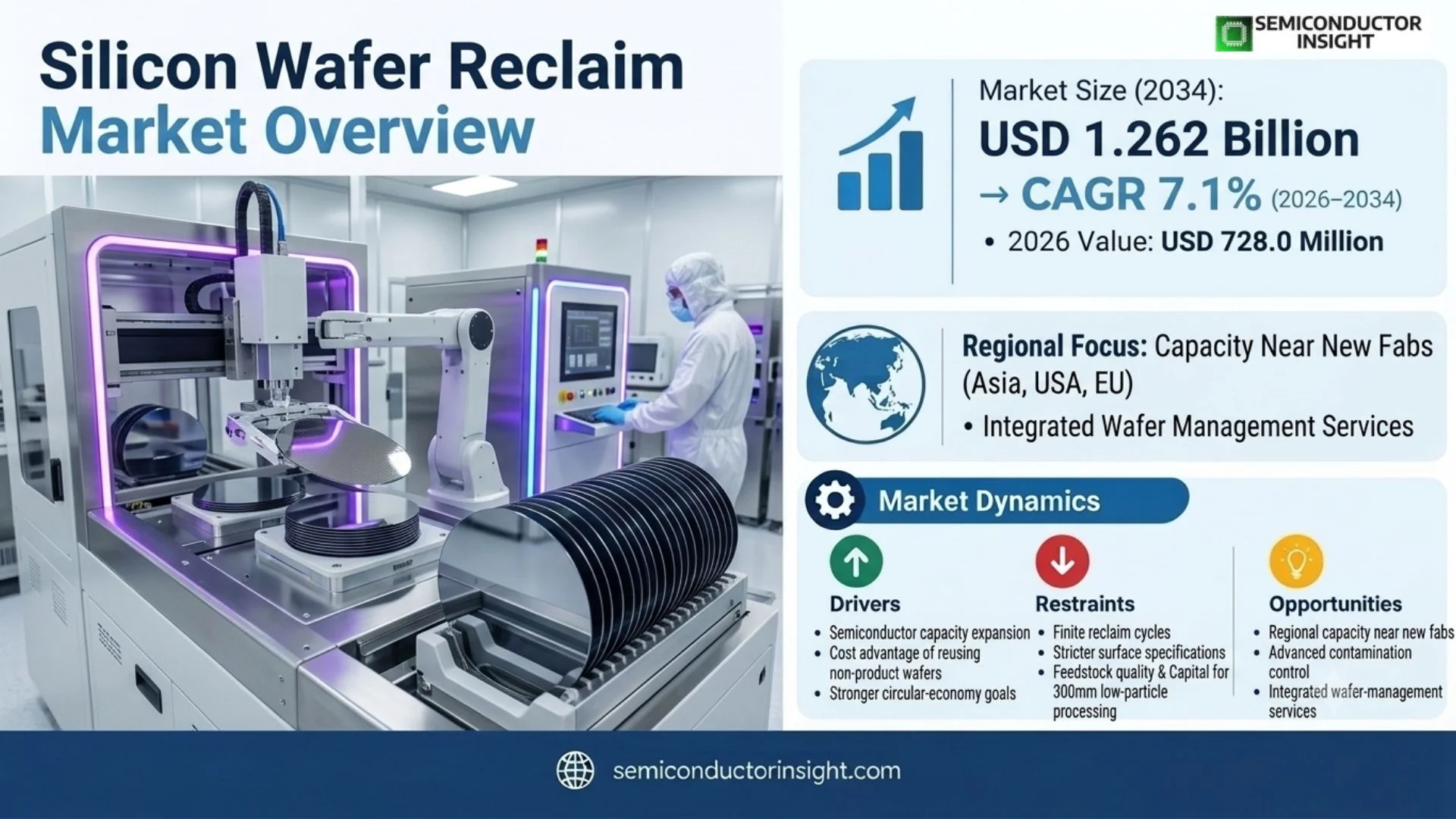
Silicon Wafer Reclaim Market was valued at USD 680 million in 2025. The market is estimated at USD 728 million in 2026 and is projected to reach USD 1.262 billion by 2034, expanding at a CAGR of 7.1% during 2026–2034. Asia Pacific remains the largest regional market.
Silicon wafer reclaim is the controlled reprocessing of used monitor, dummy and test wafers so they can return to semiconductor manufacturing for process monitoring, equipment qualification and non-device production steps. Reclaim typically removes deposited films, surface contamination and damage through stripping, etching, lapping or polishing, followed by precision cleaning, inspection and packaging. The commercial distinction from wafer recycling is that reclaim restores the wafer surface through polishing and may slightly reduce thickness, allowing repeated reuse until dimensional or surface specifications can no longer be met.
The value proposition is strongest where a fab uses large quantities of non-product wafers. Monitor and dummy wafers occupy chamber positions during process qualification, preventive maintenance, seasoning, metrology and equipment checks, but they do not need the full economics of a new prime device wafer. Reclaim therefore converts an internal waste stream into a lower-cost process-control input. RS Technologies emphasizes chemical stripping, copper decontamination and proprietary polishing to increase the number of reuse cycles, while Pure Wafer describes a controlled flow from inspection and sorting through lapping, etching, polishing and final clean.
Demand is structurally tied to semiconductor wafer starts and tool count. SEMI’s Q3 2026 300mm Fab Outlook projects global 300mm front-end equipment spending of USD 149 billion in 2026 and a 7% increase in installed 300mm capacity. New fabs and capacity expansions require extensive equipment qualification and process monitoring before reaching stable high-volume output, increasing demand for monitor and dummy wafers and eventually enlarging the feedstock pool available to reclaim suppliers. Sustainability goals strengthen the same economics by extending substrate life and reducing disposal.
Segment Analysis: By Type
By type, the market is segmented into monitor wafers and dummy wafers. Monitor wafers hold the stronger market position because they are consumed repeatedly for process-control checks, film measurements, chamber qualification and equipment monitoring. Dummy wafers remain essential for chamber filling, thermal uniformity, process stabilization and equipment setup, but their demand profile can vary more by process step and tool architecture.
| Type | Technical / commercial role | Market position |
|---|---|---|
| Monitor Wafers | Used for equipment calibration, process monitoring, film checks and qualification steps where surface quality and repeatability are required. | Largest type; high usage frequency and repeatable reclaim cycles support stable recurring volumes. |
| Dummy Wafers | Used as non-device placeholders for chamber loading, process stabilization, thermal balance and setup. | Large installed demand, especially in mature and high-volume fabs; specifications may be less stringent than monitor-grade material depending on use. |
Wafer size economics
Wafer size changes both the economics and the technical barrier to reclaim. 300mm wafers carry the highest strategic importance because they dominate advanced logic and memory production and because their larger area makes replacement with new prime or test material more expensive. 200mm remains important in analog, power, MEMS, automotive and mature-node manufacturing. Reclaim suppliers must control flatness, particles, thickness variation and metal contamination after each cycle, so capability on a nominal wafer diameter does not automatically mean qualification for every customer specification.
| Wafer Size | Market role | Qualification focus |
|---|---|---|
| 200mm | Large mature-node installed base across analog, power, MEMS and automotive applications. | Cost efficiency, surface condition, thickness and contamination control. |
| 300mm | Strategic growth segment tied to advanced logic, memory and leading foundries. | Low-particle performance, flatness, metal control and repeatability across high-volume cycles. |
| Others | Smaller diameters and specialty substrates used in legacy, research and niche applications. | Application-specific specifications and flexible batch processing. |
Segment Analysis: By Application
By application, the market is segmented into IDM, foundry and other users. Foundries lead because their scale, multi-tool manufacturing environments and constant process qualification generate large volumes of monitor and dummy wafer consumption. IDMs remain substantial users, especially in memory, analog, power and automotive semiconductors, where fabs seek the same combination of cost efficiency, controlled surface quality and waste reduction.
| Application | Demand characteristics |
|---|---|
| IDM | Integrated device manufacturers use reclaimed wafers for internal process control, equipment qualification and non-product runs. Purchasing emphasizes consistency across multiple fabs, contamination control and predictable delivery. |
| Foundry | Foundries operate large, diverse tool fleets and frequently qualify processes for many customer products. High monitor-wafer usage and strong cost discipline make reclaim a core wafer-management service. |
| Others | Research institutes, equipment makers, pilot lines and specialty fabs use reclaimed wafers for tool development, demonstrations, engineering lots and metrology work. |
Segment Analysis: By Wafer Size
The market is segmented into 200mm, 300mm and other wafer sizes. 300mm carries the strongest growth logic because global 300mm fab capacity continues to expand, while 200mm remains a durable installed base across automotive, power, analog and MEMS manufacturing. A reclaim provider’s competitive position depends on having qualified cleaning, polishing and metrology for the specific diameter and surface specification.
| Wafer Size | Demand characteristics |
|---|---|
| 200mm | Stable replacement and reclaim demand from mature-node, analog, power and MEMS fabs. |
| 300mm | Highest strategic growth, driven by foundry, logic and memory capacity additions and tighter metrology requirements. |
| Others | Niche volumes serving older fabs, R&D and specialty substrate programs. |
Segment Analysis: By Reclaim Process
The reclaim flow uses combinations of film stripping, etching, lapping, polishing and precision cleaning. CMP or equivalent precision polishing is central where the wafer must regain a mirror-like surface and tight flatness, while etching removes damaged or contaminated surface layers and specialized steps address metals and deposited films. Process integration is a competitive capability because excessive material removal shortens wafer life and weak cleaning can fail contamination specifications.
| Reclaim Process | Commercial significance |
|---|---|
| Chemical Mechanical Polishing (CMP) | Restores surface finish and flatness; process control determines material removal, yield and number of future reclaim cycles. |
| Etching | Removes films, damaged layers and contamination; chemistry selection must protect wafer geometry and downstream cleanliness. |
| Others | Lapping, grinding, stripping, precision cleaning, laser marking and metrology create a complete reclaim service flow. |
Regional Analysis
Asia Pacific dominates the silicon wafer reclaim market, supported by the concentration of foundry, memory and IDM capacity in Taiwan, South Korea, China and Japan. North America is the next strategically important growth region because new U.S. fabs expand the local monitor-wafer and reclaim-service requirement, while Europe remains a high-quality, sustainability-oriented market tied to automotive, power and specialty semiconductor production.
How does regional demand differ across the silicon wafer reclaim market?
Reclaim is unusually local for a semiconductor material service because used wafers must be collected, processed and returned with controlled turnaround time and traceability. Dense fab clusters therefore support nearby reclaim capacity. Asia Pacific has the strongest economics because wafer volumes are highest; North America is building a more resilient domestic ecosystem; Europe values circularity and high specification; South America and Middle East & Africa remain niche because front-end manufacturing capacity is limited.
| Region | Position | Growth outlook | Demand profile | Commercial selection factor |
|---|---|---|---|---|
| Asia Pacific | Largest | High | Dense fab clusters and local reclaim plants | Qualified capacity, turnaround time, particle/metal control |
| North America | Strategic growth | High | New fabs + established IDMs | Domestic capacity, low-particle performance and logistics |
| Europe | Established niche | Moderate | Automotive/power fabs + sustainability | Quality, traceability and circular-economy value |
| South America | Small | Selective | Limited local front-end activity | Imported service and logistics cost |
| Middle East & Africa | Emerging | Selective | Israel + new technology investment | Technical qualification and international service coverage |
Key Silicon Wafer Reclaim Manufacturers and Competitive Landscape
Competition is based on qualified capacity, surface quality, contamination control, allowable reclaim cycles, turnaround time and proximity to fabs. The leading suppliers operate dedicated wafer-processing plants rather than treating reclaim as a simple cleaning service. Scale matters because high-volume fabs require predictable monthly capacity, but process technology matters equally: excessive silicon removal reduces future reclaim cycles, while insufficient metal or particle removal can disqualify a wafer from process-control use.
RS Technologies provides one of the clearest public capacity benchmarks. Its 2025 annual report lists 12-inch reclaim capacity of 340,000 wafers per month at Sanbongi in Japan and 300,000 per month at Tainan in Taiwan, plus 8-inch capacity of 150,000 per month in Japan. The company also states that production began in China in 2023 and describes reclaimed wafers as its core business. These disclosures illustrate how the competitive frontier combines multi-region capacity with proprietary stripping, decontamination and polishing technology.
Phoenix Silicon International competes from Taiwan with wafer reclaim, new test wafers, thinning and other wafering services. Its corporate materials describe 6-inch, 8-inch and 12-inch reclaim capability and emphasize process monitoring, reuse and ESG benefits. Pure Wafer anchors the North American competitive set with U.S. facilities, 100mm to 300mm reclaim capability, low-particle inspection and integrated foundry, thin-film and wafer-management services.
Customer qualification creates durable relationships. A fab does not evaluate reclaimed wafers only on price; it validates particles, metals, flatness, thickness, surface finish and repeatability against its monitoring application. Suppliers that can document consistent metrology and return wafers within a predictable cycle time can protect share even when lower-cost alternatives exist.
Tier structure
| Competitive tier | Representative companies | How they compete |
|---|---|---|
| Global / regional scale leaders | RS Technologies, Phoenix Silicon International, Kinik, Mimasu Semiconductor Industry | Large qualified capacity, established foundry/IDM relationships, multi-diameter processing and advanced metrology. |
| North American and specialized service leaders | Pure Wafer, Scientech, Ferrotec, TOPCO Scientific | Regional proximity, specialized reclaim/fabrication services, 200mm/300mm capabilities and integrated wafer management. |
| Regional specialists | Hamada Rectech, GST, Xtek Semiconductor, Shinryo, KST World, Vatech, OPTIM Wafer Services | Country-level customer access, flexible services and niche process capability. |
Key companies profiled
RS Technologies, Kinik, Phoenix Silicon International, Hamada Rectech, Mimasu Semiconductor Industry, GST, Scientech, Pure Wafer, TOPCO Scientific Co. LTD, Ferrotec, Xtek semiconductor (Huangshi), Shinryo, KST World, Vatech Co., Ltd., OPTIM Wafer Services
Silicon Wafer Reclaim Production Capacity Analysis
Reclaim capacity is measured in wafers per month, but usable capacity depends on diameter, incoming-film mix, cleaning specification and required final surface quality. High-throughput plants need separate stripping, etching, polishing, cleaning and metrology tools, plus contamination-controlled material flow. A nominal 300mm line may therefore have different effective output for low-particle monitor wafers than for less demanding dummy-wafer grades.
RS Technologies disclosed 340,000 12-inch wafers per month of capacity at its Sanbongi plant and 300,000 per month at Tainan in its 2025 annual report. Sanbongi also carried 150,000 wafers per month of 8-inch capacity. The company identifies Japan, Taiwan and China as its three reclaim manufacturing bases, which provides geographic coverage close to major Asian fabs. These figures show why capacity concentration is a structural competitive factor in the market.
North America has a smaller but strategically important capacity base. Pure Wafer operates U.S. facilities serving 100mm to 300mm wafers and positions its low-particle reclaim capability around advanced semiconductor requirements. As U.S. fabs expand, local reclaim capacity becomes more valuable because transporting used wafers internationally increases cycle time, handling and inventory requirements.
| Producer / facility indicator | Publicly disclosed capability | Strategic implication |
|---|---|---|
| RS Technologies – Sanbongi, Japan | 12-inch: 340,000 wafers/month; 8-inch: 150,000 wafers/month | Large multi-diameter base supporting Japan and export customers. |
| RS Technologies – Tainan, Taiwan | 12-inch: 300,000 wafers/month | Direct access to Taiwan’s dense foundry ecosystem. |
| Pure Wafer – United States | 100mm–300mm reclaim; low-particle capability down to 19nm/26nm defect counts | High-value domestic service for U.S. IDMs, foundries and equipment customers. |
| Phoenix Silicon International – Taiwan | 6-inch, 8-inch and 12-inch reclaim services | Integrated wafering platform close to major Asia Pacific fabs. |
Silicon Wafer Reclaim Market Dynamics: Drivers, Restraints and Opportunities
Market growth is driven by semiconductor capacity expansion, the cost advantage of reusing non-product wafers and stronger circular-economy goals. Restraints arise from finite reclaim cycles, stricter surface specifications, feedstock quality and the capital required for low-particle 300mm processing. The best opportunities are in regional capacity near new fabs, advanced contamination control and integrated wafer-management services.
MARKET DRIVERS
Drivers Impact Analysis*
| Driver | Relative impact on growth | Commercial mechanism |
|---|---|---|
| 300mm fab-capacity growth | High | More tools and wafer starts increase monitor/dummy wafer consumption and future reclaim feedstock. |
| Cost reduction for non-product wafers | High | Reclaim extends substrate life and lowers the recurring cost of process control and equipment qualification. |
| Circular-economy and waste-reduction goals | Medium-High | Reuse reduces disposal and virgin-wafer demand, aligning with semiconductor sustainability programs. |
| New U.S. and regional fab clusters | Medium-High | Localized manufacturing increases demand for nearby qualified reclaim capacity and faster logistics. |
Fab expansion increases monitor-wafer consumption
SEMI projects installed 300mm capacity to rise 7% in 2026 while front-end equipment spending reaches USD 149 billion. New tools require substantial qualification, seasoning, metrology and process-monitoring activity before stable production, all of which consumes non-product wafers. As these wafers cycle out of specification for a given use, they become reclaim feedstock, creating a direct link between fab investment and reclaim demand.
Reclaim lowers recurring process-control cost
Monitor and dummy wafers do not generate saleable die, yet they are essential to fab operation. Reclaim restores used wafers for additional cycles instead of replacing them with new test or prime-grade material. RS Technologies specifically positions proprietary polishing around increasing the number of times a wafer can be reclaimed, showing that customer value is created by maximizing lifetime while maintaining required cleanliness and geometry.
Sustainability strengthens the economic case
Reclaim extends the useful life of a high-purity silicon substrate and reduces the number of wafers discarded after monitoring use. This circular model aligns cost reduction with waste minimization, which makes it easier for fabs to incorporate reclamation into formal sustainability programs. RS Technologies publishes declining water and energy use per thousand reclaimed wafers through 2025, indicating that process efficiency itself is also becoming part of supplier competitiveness.
MARKET RESTRAINTS
Restraints Impact Analysis*
| Restraint | Relative impact on growth | Commercial mechanism |
|---|---|---|
| Finite wafer thickness and reclaim cycles | High | Each polishing cycle removes silicon, eventually making a wafer too thin or geometrically unsuitable for further reuse. |
| Stricter particle and metal specifications | High | Advanced fabs require tighter inspection and contamination control, increasing processing cost and rejection risk. |
| Feedstock variability | Medium-High | Incoming films, scratches, metals and prior process history affect yield and determine whether a wafer can be reclaimed. |
| Geographic logistics | Medium | Used wafers must move securely between fab and reclaimer, favoring suppliers located near dense fab clusters. |
Every wafer has a finite reclaim life
Polishing and surface restoration remove material. After repeated cycles, thickness, edge geometry or flatness can fall outside the customer’s specification, ending the wafer’s usable reclaim life. This means suppliers cannot create unlimited output from the same installed wafer base and must continuously manage incoming feedstock quality and removal depth.
Advanced-node monitoring raises inspection difficulty
As process-control requirements tighten, reclaimed wafers need lower particle counts, stronger metal decontamination and more uniform surfaces. Pure Wafer advertises low-particle reclaim inspection down to 19nm and 26nm defect counts, illustrating the metrology burden. Capability at this level requires advanced cleaning, inspection and process control, raising capital and operating cost.
Feedstock condition creates yield variability
A used wafer may arrive with metals, thick films, scratches, haze or damage that makes economical reclamation difficult. Suppliers therefore sort incoming material before processing and may route wafers through different strip, etch, lap or polish flows. Variable incoming condition complicates throughput planning and can reduce effective plant capacity during periods of aggressive fab processing.
MARKET OPPORTUNITIES
Local reclaim capacity around new U.S. fabs
CHIPS-backed fab construction in Arizona, New York and other U.S. locations enlarges the domestic monitor-wafer pool. Reclaim providers with qualified 300mm capacity can reduce transport time, inventory and supply risk for customers that prefer an in-region circular wafer loop.
Advanced precision cleaning and contamination control
Pure Wafer announced Precision Surface Cleaning in 2026 for semiconductor and quantum applications. Similar technology that removes atomic-scale contamination while preserving substrate geometry can raise reclaim yield and extend the use of reclaimed wafers into more demanding process-control applications.
Integrated wafer-management services
Customers benefit when reclaim is combined with inventory tracking, wafer brokerage, thin films, test wafers and logistics. A broader service platform reduces internal handling and allows fabs to optimize when to reclaim, recycle or replace a wafer, creating value beyond the unit processing fee.
200mm and specialty-node resilience
Although 300mm drives growth, 200mm remains deeply installed in power, analog, MEMS and automotive manufacturing. Suppliers that maintain efficient 200mm lines can capture recurring demand where mature fabs operate for many years and cost sensitivity makes reclaimed monitor wafers particularly attractive.
Silicon Wafer Reclaim Supply Chain Analysis
Used monitor/dummy wafer collection
Film strip, etch, lap and polish
Precision clean, metrology and classification
Return logistics and reuse in fab
The supply chain begins inside the fab, where used monitor and dummy wafers are sorted by diameter, material history, thickness and surface condition. Wafers with damage or unsuitable process history may be rejected before reclaim. Traceability matters because contamination risk depends on what films, metals and chemistries were previously present.
Processing then removes films and restores the silicon surface. RS Technologies highlights proprietary stripping, copper decontamination and polishing; Pure Wafer describes inspection, lapping, etching, polishing and advanced cleaning. The objective is to remove only the material necessary to meet specification because excessive silicon loss shortens the number of future reclaim cycles.
Final cleaning and metrology determine whether the wafer can return to service. Particle counts, total thickness variation, flatness, metals and visual defects are checked against customer specifications. Qualified wafers are packed in contamination-controlled cassettes and returned with documentation. The economic advantage depends on high yield, repeatable quality and short cycle time across this closed-loop flow.
Recent Developments in the Silicon Wafer Reclaim Market
6 May 2026 – Pure Wafer launches Precision Surface Cleaning
Pure Wafer announced a new process-integrated precision surface cleaning capability for semiconductor manufacturing and quantum sensing, targeting contamination challenges associated with sub-10nm devices, advanced architectures and emerging materials. The development expands the technical ceiling for reclaim and wafer-service providers. Source
27 Mar 2026 – RS Technologies publishes expanded reclaim-capacity profile
RS Technologies’ 2025 annual report disclosed reclaim production across Japan, Taiwan and China, including 340,000 12-inch wafers per month in Japan and 300,000 per month in Taiwan. The company also reported a 33% market-share position as its own long-term-vision benchmark. Source
Jan 2025 – Phoenix Silicon International breaks ground for new Taichung branch fab
PSI’s corporate record lists a January 2025 groundbreaking ceremony for a new Taichung branch fab, consistent with ongoing expansion of Taiwan’s wafer-processing and semiconductor-service infrastructure. Source
REPORT SCOPE & SEGMENTATION
| Report Title | Silicon Wafer Reclaim Market Size, Share & Industry Analysis, By Type (Monitor Wafers, Dummy Wafers), By Application (IDM, Foundry, Others), By Wafer Size (200mm, 300mm, Others), By Reclaim Process (Chemical Mechanical Polishing (CMP), Etching, Others), and Regional Forecast, 2026-2034 |
| Base / Estimated / Forecast Years | 2025 / 2026 / 2034 |
| Market Size | USD 680 million in 2025; USD 728 million in 2026; USD 1.262 billion by 2034 |
| Forecast CAGR | 7.1% during 2026–2034 |
| Regional Coverage | North America, Europe, Asia Pacific, South America, Middle East & Africa |
| By Type | Monitor Wafers; Dummy Wafers |
| By Application | IDM (Integrated Device Manufacturers); Foundry; Others |
| By Wafer Size | 200mm; 300mm; Others |
| By Reclaim Process | Chemical Mechanical Polishing (CMP); Etching; Others |
| Key Companies Profiled | RS Technologies, Kinik, Phoenix Silicon International, Hamada Rectech, Mimasu Semiconductor Industry, GST, Scientech, Pure Wafer, TOPCO Scientific Co. LTD, Ferrotec, Xtek semiconductor (Huangshi), Shinryo, KST World, Vatech Co., Ltd., OPTIM Wafer Services |
Frequently Asked Questions
What is the current size of the silicon wafer reclaim market?
Silicon wafer reclaim market is estimated at USD 680 million in 2025, rising to USD 728 million in 2026 and projected to reach USD 1.262 billion by 2034, representing a 7.1% CAGR during 2026–2034.
What is a reclaimed silicon wafer?
A reclaimed silicon wafer is a used monitor, dummy or test wafer that has been stripped of films, resurfaced through etching, lapping or polishing, precisely cleaned and inspected so it can be reused for process monitoring, equipment qualification or other non-product fab operations.
Which wafer type leads the market?
Monitor wafers hold the leading position because fabs consume them frequently for process measurements, chamber checks and equipment calibration. Their recurring use creates a steady return stream suitable for multiple reclaim cycles when thickness and surface condition remain within specification.
Which application is largest?
Foundries are the leading application because large multi-customer fabs operate extensive tool fleets and conduct continuous process qualification. IDMs are also major users, particularly in memory, analog, power and automotive semiconductor manufacturing.
Which wafer size offers the strongest growth opportunity?
300mm is the most strategic growth segment because advanced logic, foundry and memory capacity continues to expand. SEMI projects installed 300mm capacity to rise 7% in 2026, increasing both demand for monitor wafers and the future pool of wafers available for reclamation.
Which region dominates the market?
Asia Pacific is the dominant region. The report scope places it above 60% of global consumption volume, supported by the concentration of semiconductor manufacturing and reclaim capacity in Taiwan, South Korea, China and Japan.
Who are the key silicon wafer reclaim companies?
Key profiled companies include RS Technologies, Kinik, Phoenix Silicon International, Hamada Rectech, Mimasu Semiconductor Industry, GST, Scientech, Pure Wafer, TOPCO Scientific, Ferrotec, Xtek Semiconductor, Shinryo, KST World, Vatech and OPTIM Wafer Services.
What are the main barriers to wafer reclaim growth?
The principal barriers are finite wafer thickness, incoming-feedstock variability, stricter particle and metal contamination limits, and the need for costly low-particle 300mm processing and metrology. These factors determine how many wafers can be economically restored to a customer’s specification.
Research Sources & Evidence Base
Get Sample Report PDF for Exclusive Insights
Report Sample Includes
- Table of Contents
- List of Tables & Figures
- Charts, Research Methodology, and more...