Key Statistics
Key Takeaways
- Revenue trajectory: the global market reached USD 216 million in 2026 and is forecast to attain USD 2,474 million by 2036, representing 27.6% annual growth over the 2027–2036 period; the estimate concerns outsourced silicon-carbide device wafer processing rather than sales of finished inverters.
- Technology mix: SiC MOSFET foundry processing leads the type split with an estimated ~78% of 2026 revenue, reflecting more complex mask sets, implantation, gate oxide and reliability qualification than the ~22% share of Schottky barrier diode processing.
- End-use demand: automotive and EV/HEV programmes account for an estimated ~51% of foundry-service revenue, with charging systems contributing ~13% and photovoltaic, storage and wind power another ~20%; OEM qualification cycles determine when designs become recurring wafer orders.
- Regional leadership: Asia-Pacific holds an estimated ~49% of revenue, supported by Taiwanese specialty foundries and China-based device manufacturing, while North America represents ~22% because X-FAB operates a 150mm SiC foundry in Lubbock, Texas.
- Operational bottleneck: gate-oxide reliability, defect density and wafer-level yield remain the largest process challenges, while moving from 150mm to 200mm substrates changes equipment qualification and customer design rules rather than automatically creating saleable die.
SiC Foundry Service Market Overview
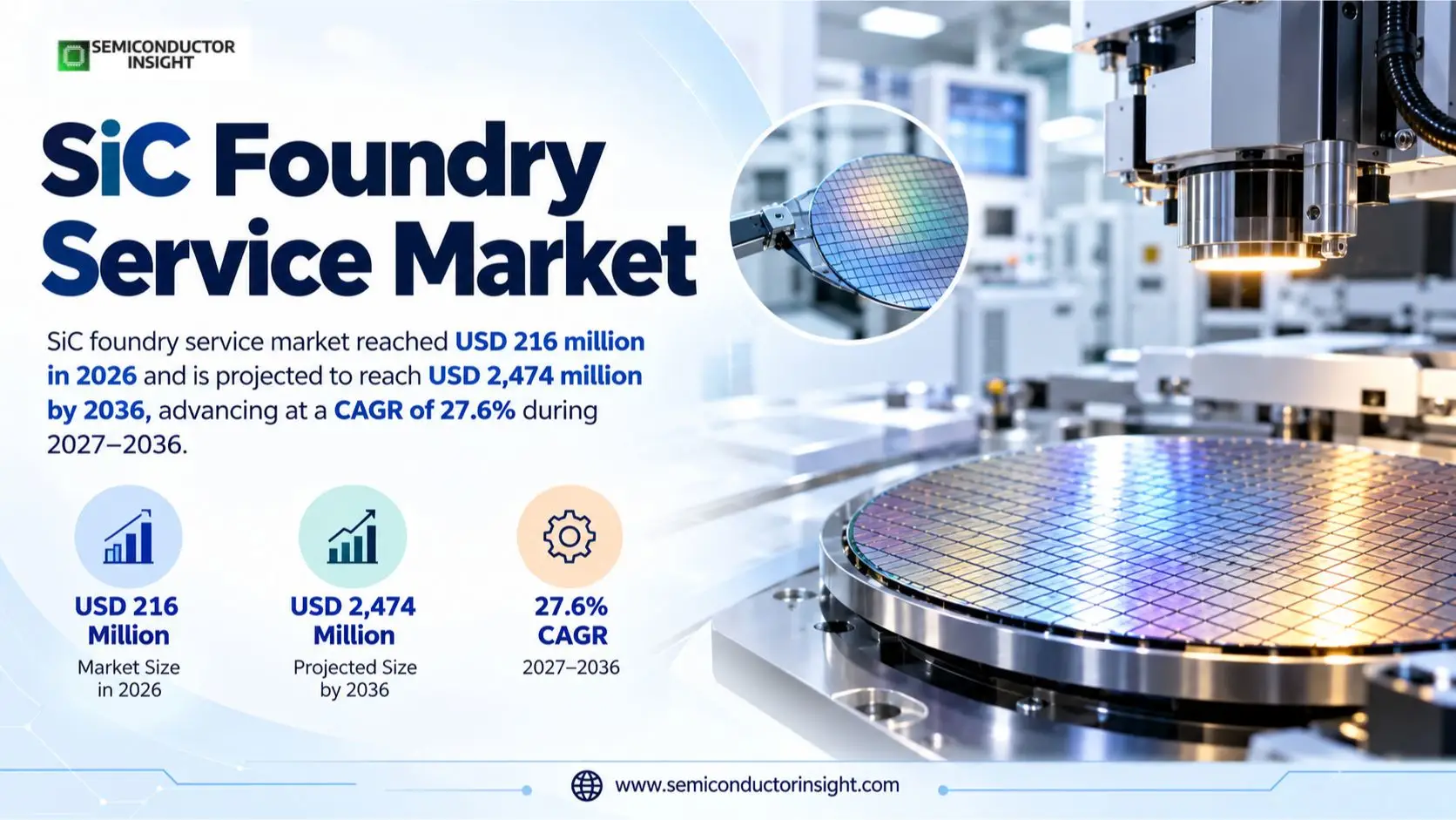
SiC foundry service market reached USD 216 million in 2026 and is projected to reach USD 2,474 million by 2036, advancing at a CAGR of 27.6% during 2027–2036. Asia-Pacific was the largest regional market in 2026 with an estimated ~49% share, reflecting the concentration of merchant wafer processing and power-device supply chains in Taiwan and China.
Silicon-carbide foundry services turn customer-supplied power-device designs into patterned, processed semiconductor wafers. A specialist fabricator carries out epitaxial preparation where contracted, lithography, high-temperature ion implantation, annealing, gate dielectric formation, metallization, backside processing and wafer-level electrical testing. These activities demand process control beyond conventional silicon because SiC crystal defects, interface traps and thermal budgets can impair MOSFET threshold stability or diode leakage. Merchant foundries sell engineering lots, qualified wafer starts and production runs to fabless designers and integrated device makers seeking external capacity.
The market boundary includes contract SiC MOSFET and Schottky barrier diode wafer fabrication, process development, mask and qualification services that are charged as part of foundry engagements, and customer-directed wafer-level manufacturing. It does not count merchant bare-substrate sales, standalone epitaxial wafers sold to unrelated customers, packaging revenue, finished modules, or complete vehicle inverters. The distinction matters because a vertically integrated company may report material, device and module revenue together; only its qualifying external fabrication services belong in this revenue pool. Prototyping and pilot wafer runs are included where customers pay the foundry.
Commercial capability is concentrated among relatively few providers. X-FAB processes 150mm SiC wafers at its Lubbock, Texas site and provides modular process blocks through XbloX; EpiSil describes 100mm and 150mm dedicated SiC lines for Schottky diodes and MOSFETs in Taiwan. Sanan IC markets SiC device solutions in China, while STMicroelectronics and Sanan announced a dedicated 200mm joint venture for ST products in Chongqing. Such dedicated captive or single-customer arrangements influence industry capacity but should not be confused with broadly accessible merchant foundry revenue.
External demand follows electrification, but it does not move in a straight line with electric-car registrations. The International Energy Agency counted more than 20 million electric cars sold worldwide in 2025, a 20% annual increase, yet wafer starts depend on whether vehicle platforms use SiC, how many devices each inverter requires, how large each die is and what fraction of manufacturing is outsourced. Design wins can precede meaningful wafer revenue by several quarters because automotive customers validate reliability and supplier change controls before authorizing production.
The production economics are moving toward larger wafer diameters and tighter process standardization. X-FAB said its XSICM03 platform can improve die-per-wafer output by up to 30% relative to its preceding planar cell design, while Wolfspeed launched a commercial 200mm materials portfolio in September 2025. The wafer-area advantage of 200mm over 150mm is substantial, but defect mapping, wafer bow, oxide stability and back-end tool compatibility determine realized cost per good die. Merchant foundries therefore compete on qualified yields and repeatable cycle times rather than advertised substrate diameter alone.
Beyond vehicles, solar inverters, stationary storage, industrial motor drives and high-efficiency server power conversion broaden the addressable customer base. The IEA reported solar PV additions above 600 GW in 2025, and its Renewables 2025 outlook projects about 4,600 GW of renewable power additions over 2025–2030. These are downstream equipment indicators, not direct measures of SiC foundry sales. They nevertheless explain why device designers seek foundry partners capable of supporting both automotive qualification and industrial product variants without duplicating costly fabrication infrastructure.
Segment Analysis: By Type
By device process, SiC MOSFET and SiC SBD are the two published type segments. MOSFET fabrication represents an estimated ~78% of 2026 foundry-service revenue and has a modeled ~28.4% growth trajectory, while SBD fabrication accounts for ~22% and remains important for lower-complexity power conversion and freewheeling applications. These are shares of outsourced processing fees, not shares of all silicon-carbide device sales.
| Type | Foundry process requirements | Competitive and demand implications |
|---|---|---|
| SiC MOSFET | Fabrication requires multi-layer lithography, selective implantation, activation anneals, carefully grown gate oxide, contacts and backside metallization. Device variants include planar and trench designs, with different oxide field profiles and reliability requirements. The foundry must translate customer cell geometries into repeatable process windows and provide traceable wafer-level parametric test data across lots. | Largest 2026 type (~78%). Automotive and high-voltage industrial customers value low on-resistance and stable gate thresholds, making MOSFET flows more process-intensive and commercially valuable. X-FAB XbloX standardizes proven process modules to reduce the design-to-fab cycle, but each customer still needs mask, layout and long-term reliability qualification before moving from pilot wafers to repeat orders. |
| SiC SBD | Schottky barrier diode manufacturing uses patterned junction and termination structures, contact metals, passivation and backside operations, with leakage, blocking voltage and thermal robustness as key acceptance criteria. Relative to MOSFETs, there is no gate dielectric to qualify, although edge termination, defect-related leakage and surface cleanliness remain demanding for high-voltage devices. | Estimated ~22% of 2026 processing revenue. Diodes are used in PFC stages, fast switching power supplies and selected inverter designs, and are often an entry technology for a foundry expanding into SiC. Customers still need consistent barrier height and leakage performance, while process simplification makes wafer pricing more competitive and creates pressure to distinguish providers through yield and delivery reliability. |
SiC MOSFET Foundry Processing
The MOSFET route starts with epitaxial material acceptance and progresses through implants, anneals, oxide growth, patterned gates and contacts. A process that performs well on a small engineering lot may still need multiple iterations before it can maintain low leakage and tight threshold distributions across a production campaign. X-FAB developed XSICM03 to reduce cell pitch by more than 25%, enabling up to 30% more dies per wafer; the commercial benefit depends on whether the customer can retain blocking voltage and oxide lifetime at the smaller geometry.
Foundry customers compare the process design kit, wafer map data, cycle-time commitments and qualification documentation rather than the quoted wafer-start fee alone. Automotive programmes demand change control over tools and chemicals, and a second-source strategy may require deliberate compromises in cell layout to preserve manufacturability at two sites. In the 2026 model, MOSFET services lead because high-voltage traction and industrial designs generate more engineering and production steps than diode products.
SiC Schottky Barrier Diode Foundry Processing
SBD foundry services address diode structures that suppress reverse-recovery losses in power-factor correction, auxiliary converters and selected energy systems. Device designers specify barrier metallurgy, junction termination, forward drop and leakage at elevated temperature; foundries must then hold those characteristics across substrate lots whose defect densities vary. This product family can help a customer qualify a new foundry relationship before committing a more complex MOSFET technology to the same manufacturing line.
Although SBD process flows are shorter, high-voltage products remain sensitive to epitaxial thickness and surface defects. EpiSil advertises verified SiC Schottky and MOSFET platforms and equipment including high-temperature implant and anneal tools, demonstrating the shared infrastructure between the two families. SBD foundry growth remains positive as charging, solar and industrial power stages expand, but value capture per processed wafer is generally lower than for advanced MOSFET flows.
Segment Analysis: By Application
Application demand is led by Automotive & EV/HEV with an estimated ~51% of 2026 revenue, followed by PV, Energy Storage and Wind Power (~20%), EV Charging (~13%), UPS, Data Center and Server (~9%) and Others (~7%). The five segments describe the final use of foundry-processed SiC device wafers rather than the location of the fabrication plant.
| Application | Demand characteristics |
|---|---|
| Automotive & EV/HEV | Largest segment (~51%). Traction inverters, on-board chargers and vehicle power distribution require reliable high-voltage MOSFETs and selected diodes. The IEA recorded more than 20 million electric cars sold in 2025, but qualification lead times and customer insourcing strategies determine foundry orders. Vehicle programmes create attractive multiyear wafer demand after approval and require strict lot traceability, process-change notification and low defectivity. |
| EV Charging | Estimated ~13% share. High-power charging stations use SiC switches and diodes in AC-DC and DC-DC conversion, with growing emphasis on power density, cooling and efficiency. Merchant foundries serve fabless designers seeking 650V, 1200V and higher-voltage devices, although charging infrastructure investment is project-based and can create uneven quarterly wafer orders. Reliability and thermal cycling performance remain central acceptance criteria. |
| UPS, Data Center & Server | Estimated ~9% share. Uninterruptible power supplies and high-density server power architectures reward low switching losses and efficient high-voltage conversion. The acquired SiC JFET portfolio announced by onsemi in January 2025 illustrates the widening technology mix for data-center power stages. This market favors designs that can be qualified rapidly and supplied consistently as server architectures change, although GaN and advanced silicon remain strong alternatives at lower voltages. |
| PV, Energy Storage, Wind Power | Estimated ~20% share. Solar string inverters, battery storage converters and wind power systems need power devices with high conversion efficiency and long operating life. The IEA reported solar PV additions exceeding 600 GW in 2025, supporting a growing installed base of inverter systems that will be built, upgraded and replaced. Device mix varies by inverter topology, and foundry suppliers must balance high-voltage capability with price sensitivity in utility-scale tenders. |
| Others | Estimated ~7% share. Industrial motor drives, railway auxiliary power, telecom equipment and specialized medical power systems create diverse but smaller design programmes. Many customers cannot justify owning a dedicated SiC fab and therefore value foundries that accept moderate-volume mask sets and offer flexible engineering support. Order sizes can be smaller than automotive volumes, but technical requirements often create durable customer relationships once qualification is complete. |
Application mix also influences how foundries allocate engineering capacity. Automotive device qualification may occupy process and reliability teams for many months before volume starts, whereas industrial power designers can use an established process platform to enter production sooner. By serving several end markets, a foundry can smooth utilization when vehicle platforms are delayed, but it must prevent customer-specific process changes from degrading the yield of other designs sharing the same implantation, annealing or oxide tools.
Regional Analysis
Asia-Pacific is the largest SiC foundry service market with an estimated ~49% of 2026 revenue, followed by North America (~22%), Europe (~21%), the Middle East and Africa (~5%) and South America (~3%). The region shares reflect merchant process capacity, device-design customers and outsourced wafer contracts rather than downstream EV registrations alone. Asia-Pacific has the strongest projected regional CAGR at ~29.2%, supported by Taiwan-based foundry expertise and the build-out of China-based SiC device capacity.
How do regional manufacturing footprints shape SiC foundry demand?
The geographic split is governed by where customers contract device processing and where fabs can qualify the relevant wafer technology. A wafer may be designed in Europe, processed in Taiwan, assembled in Southeast Asia and installed in a Chinese vehicle, so end-market sales alone cannot locate foundry revenue. Asia-Pacific benefits from Taiwan and mainland China process ecosystems; North America from X-FAB Lubbock and fabless power-device design; Europe from automotive engineering and captive SiC investment; smaller regions rely more heavily on external foundry relationships.
| Region | Position | Growth outlook | Demand profile | What decides supplier selection |
|---|---|---|---|---|
| Asia-Pacific | Largest (~49%) | Fastest (~29.2% CAGR) | Taiwan and China fab ecosystem | Qualified MOSFET platforms, local substrate access and 150mm-to-200mm transition |
| North America | Second (~22%) | Strong (~25.4% CAGR) | Lubbock foundry and US design base | Automotive process traceability and scalable engineering lots |
| Europe | Third (~21%) | Strong (~26.2% CAGR) | Automotive design and SiC integration | Qualification portability and stable supply contracts |
| Middle East & Africa | Fourth (~5%) | Developing (~26.8% CAGR) | Energy infrastructure end users | Access to overseas qualified foundries and regional power-system integrators |
| South America | Fifth (~3%) | Emerging (~28.4% CAGR) | Renewables and industrial equipment | Imported power device designs, distributor qualification and financing |
Key SiC Foundry Service Manufacturers and Competitive Landscape
The SiC foundry-service field is more specialized than the broad power-semiconductor supplier universe. X-FAB and EpiSil advertise contract wafer-processing platforms, while Sanan IC and several Chinese producers supply device manufacturing capabilities. Competitive differentiation comes from qualified MOSFET process modules, substrate supply agreements, high-temperature equipment, automotive reliability records and the ability to move a customer from engineering lots to stable production without repeated mask redesign.
X-FAB is an important reference for the independent foundry model. Its Lubbock site operates 150mm SiC wafer processing, and the XbloX platform combines reusable process blocks with a structured onboarding route. The company said in December 2025 that this approach can bring some customer production starts forward by as much as nine months compared with traditional development pathways. Such claims are process-development indicators rather than market-share disclosures, but they show why fabless customers may pay for a proven platform instead of funding an entirely custom integration flow.
EpiSil offers a different competitive advantage through its Taiwanese process base. Its published capabilities include dedicated SiC high-temperature annealing, implantation, gate oxide, wafer thinning and backside laser annealing, as well as qualified Schottky diode and MOSFET processes. That range can help customers manage both early device evaluation and outsourced production within a single organization. EpiSil-Precision separately provides SiC epitaxial materials, highlighting the importance of distinguishing a foundry fee from an upstream wafer or epitaxy sale when assessing revenue.
Sanan IC, HLMC, GTA Semiconductor, Beijing Yandong Microelectronics, United Nova Technology, Global Power Technology, Wuhu Tus-Semiconductor and AscenPower appear in the publisher competitive set. Their public roles and levels of open merchant access are not identical. Some operate integrated manufacturing, some serve specific customers or product categories, and some have limited English-language technical disclosure. A supplier should therefore be assessed on demonstrated SiC process capabilities and contract accessibility rather than simply being listed alongside a specialist foundry.
The 200mm transition is creating a second layer of competition. Materials producers such as Wolfspeed enable larger wafers, while integrated manufacturers including STMicroelectronics and Infineon invest in their own device lines. These investments may improve the availability of qualified equipment and skilled engineers but can also keep the most attractive high-volume automotive programmes captive. Merchant foundries must win with engineering flexibility, cost per qualified die and second-source resilience rather than treating every announced integrated fab as addressable external service capacity.
Tier structure
| Tier | Companies | Basis of competition |
|---|---|---|
| Dedicated merchant platforms | X-FAB; EpiSil Technology | These providers openly describe contract process platforms for SiC MOSFET and diode designs, including engineering support, automotive-oriented process controls and wafer-level manufacturing. Their commercial advantage is the ability to serve multiple unrelated device designers, although capacity and qualification schedules constrain how quickly new projects can scale. |
| Regional manufacturing providers | Sanan IC; HLMC; GTA Semiconductor; Beijing Yandong Microelectronics; United Nova Technology | These companies participate in Asian semiconductor fabrication and SiC-related manufacturing ecosystems, but service scope and access conditions differ by plant and product. Buyers need to verify exact wafer diameter, oxide reliability data, mask compatibility and whether the provider accepts merchant wafer starts or mainly manufactures for affiliated customers. |
| Specialist and adjacent participants | Global Power Technology; Wuhu Tus-Semiconductor; AscenPower; STMicroelectronics–Sanan joint venture | The publisher includes these names in its competitive set, yet some operate in device supply, captive production or related parts of the SiC chain. Their presence signals competitive pressure and manufacturing depth; it does not automatically mean that all corporate revenue or every fab line is available for third-party foundry contracts. |
Key companies profiled
- X-FAB
- EpiSil Technology Inc.
- Sanan IC
- HLMC
- GTA Semiconductor Co., Ltd.
- Beijing Yandong Microelectronics
- United Nova Technology
- Global Power Technology
- Wuhu Tus-Semiconductor
- AscenPower
SiC Foundry Service Production Capacity and Process Capability
Foundry capacity is measured by qualified wafer starts, yield and process availability rather than nominal cleanroom area alone. Most merchant programmes use 150mm SiC wafers, while 200mm substrates and process lines are being qualified across the industry. Larger diameters offer potential die-cost advantages, but customer mask transfer, implantation uniformity, defect control and gate-oxide reliability must be proven before a nominal capacity increase translates into commercially useful output.
At X-FAB’s Lubbock operation, the SiC foundry platform is organized around established 150mm process modules and an automotive-oriented quality system. The company has invested in internal epitaxy to manage a sensitive upstream step and reduce dependence on third-party lead times. Its annual reporting describes capacity expansion and rising prototyping activity, but total wafer starts across the group include other technologies and must not be interpreted as SiC merchant output. Foundry capacity relevant to customers is the number of qualified wafers that can run on their exact process route.
Taiwanese providers such as EpiSil maintain dedicated equipment for the unusually high temperatures required by SiC activation and gate oxide formation. Implant uniformity, surface preparation, defect mapping and backside metal adhesion can all constrain the number of acceptable die per wafer. A foundry with more tool hours may still deliver fewer qualified chips if process integration is unstable, so device designers compare parametric distributions and long-term reliability evidence before committing to production allocations.
The industry is preparing for 200mm wafers, and Wolfspeed’s September 2025 materials launch demonstrates commercial substrate availability. Yet the diameter transition can expose wafer bow, thickness variation and equipment handling problems that are less visible at 150mm. Successful migration requires coordinated materials specifications, compatible lithography and metrology, and new yield learning across many lots. Foundries that manage the transition without disrupting existing customer qualifications can improve throughput and pricing competitiveness over the 2027–2036 horizon.
SiC Foundry Service Market Dynamics: Drivers, Restraints and Opportunities
Merchant SiC wafer-processing demand grows when device designers outsource more high-voltage fabrication and when foundries shorten qualification cycles without sacrificing reliability. Electric vehicles, renewable conversion and higher-density power supplies expand the device pipeline, while process defectivity, customer insourcing, wafer-material costs and uneven fab utilization restrain the pace of recognized service revenue.
MARKET DRIVERS
Drivers Impact Analysis*
| Market Drivers | Impact Rank | CAGR Contribution (%) | 2027–2029 | 2030–2032 | 2033–2036 |
|---|---|---|---|---|---|
| Automotive SiC MOSFET design wins | High | +12.00% | High | High | Medium |
| Qualified merchant capacity and customer outsourcing | High | +8.00% | High | High | High |
| Solar, storage and industrial power conversion | Medium-High | +6.00% | Medium | High | High |
| 200mm materials and wafer yield improvement | Medium | +4.80% | Medium | High | High |
| Others (charging and data-center power designs) | Low | +2.20% | Medium | Medium | High |
Electric vehicle powertrains create a recurring MOSFET wafer pipeline
Traction inverter platforms increasingly use SiC devices to reduce switching losses and cooling requirements, but the foundry revenue opportunity depends on how much fabrication is outsourced. The IEA recorded more than 20 million electric cars sold in 2025, and device designers need automotive-grade oxide reliability, traceable wafers and repeatable electrical parameters before they can ship at vehicle volumes. A foundry that wins an approved design may receive orders across several model years, giving automotive programmes an outsized effect on long-term service utilization.
Modular process platforms reduce the cost of external manufacturing
Fabless designers often lack the capital and process engineers to build a dedicated SiC line, while integrated device makers may need second-source capacity. X-FAB’s XbloX platform provides reusable process blocks and customer onboarding support, and its December 2025 announcement highlighted faster routes from evaluation to production. Standardization allows a foundry to amortize tool recipes and reliability work across multiple customers, raising the commercial value of qualified process services even when each individual customer buys a modest number of wafers.
Renewable power and storage broaden demand beyond vehicles
Solar inverters, battery storage converters and industrial power systems require efficient high-voltage switches and diodes. The IEA reported solar PV additions above 600 GW in 2025 and forecasts major renewable expansion through 2030, which supports a growing base of power conversion equipment. This end-market evidence does not directly measure foundry sales, but it increases the range of SiC device designs under development and creates opportunities for merchant fabs with flexible process and voltage options.
Larger wafer materials improve long-term manufacturing economics
Wolfspeed’s commercial 200mm SiC materials release in September 2025 marked an important input-side milestone for device manufacturers. More die can fit on a 200mm wafer than on a 150mm wafer, provided usable yield is maintained, and that potential encourages foundries to invest in compatible processing. The benefit is not immediate: implantation, gate oxide, wafer bow and inspection tools require qualification, but providers that master the transition can support higher-volume contracts and more competitive cost per die.
Charging and high-density power architectures add design diversity
Fast chargers, uninterruptible power supplies and server power systems create additional demand for high-efficiency SiC switches. onsemi’s January 2025 acquisition of a SiC JFET technology portfolio illustrates how the device family is broadening beyond standard MOSFETs and diodes. Merchant fabs benefit when these designs require specialized process development, although different voltage and topology choices mean the opportunity is distributed across many smaller programmes rather than one uniform wafer product.
MARKET RESTRAINTS
Restraints Impact Analysis*
| Market Restraints | Impact Rank | CAGR Contribution (%) | 2027–2029 | 2030–2032 | 2033–2036 |
|---|---|---|---|---|---|
| High defect and gate-oxide qualification costs | High | -2.80% | High | High | Medium |
| Captive fabrication and uneven merchant utilization | Medium-High | -2.10% | High | Medium | Medium |
| Others (material supply and price pressure) | Low | -0.50% | Medium | Medium | Low |
Defectivity and oxide reliability raise qualification cost
SiC device fabrication requires unusually tight control of crystal defects, gate interfaces and high-temperature steps. A wafer that meets dimensional specifications may still produce unacceptable leakage, threshold drift or low die yield after fabrication. Customers therefore demand extended reliability testing, process monitoring and documented corrective action before approving a foundry, which increases engineering expense and delays the conversion of development work into repeat manufacturing revenue.
Captive SiC fabs limit merchant participation in high-volume programmes
Large integrated suppliers are investing in internal 200mm SiC manufacturing and sometimes use dedicated joint ventures rather than open merchant foundries. STMicroelectronics and Sanan announced a Chongqing plant intended to manufacture ST products, illustrating how a major automotive customer can reserve capacity within a controlled supply chain. Independent foundries still serve fabless and overflow demand, but they cannot assume that every increase in global SiC device production creates an equivalent increase in outsourced service fees.
Substrate cost and utilization swings constrain profitability
SiC substrates remain technically demanding inputs, and material quality can change how many wafers pass the foundry’s process gates. When customer EV programmes are delayed, expensive implantation, epitaxy and metrology tools may operate below planned utilization, raising fixed cost per processed wafer. Price pressure from integrated suppliers and competing foundries can compound the effect, especially for simpler Schottky diode processes with fewer opportunities to differentiate through proprietary integration.
MARKET OPPORTUNITIES
Second-source process transfer for automotive customers
Vehicle and industrial customers increasingly evaluate whether critical power devices can be manufactured at more than one qualified site. A merchant foundry that documents mask rules, gate oxide performance, wafer-level test methods and change control can position itself as an independent second source. This opportunity is most attractive when an existing supplier is captive or geographically concentrated, although true transferability still requires new reliability data rather than a simple copy of the design files.
Engineering-lot services for emerging SiC device architectures
New MOSFET cell layouts, high-voltage diodes and specialized power switches often begin as low-volume wafer experiments. Foundries can charge for process development, mask tooling and qualification runs before a customer reaches mass production, diversifying revenue beyond wafer starts. The commercial challenge is to standardize enough process blocks to keep engineering margins positive while retaining flexibility for differentiated customer intellectual property and device geometry.
200mm readiness and defect-management expertise
As commercial 200mm substrates become available, foundries have an opportunity to qualify process routes that preserve die yield and reliability on larger wafers. Customers will pay attention to uniformity, wafer bow, oxide stress and metrology evidence rather than diameter claims alone. Providers with proven materials partnerships and a disciplined transfer programme can win projects that need a long-term cost roadmap without forcing designers to establish their own 200mm fabrication infrastructure.
Solar and storage customers seeking tailored high-voltage devices
Power conversion equipment makers may need specific switching, leakage or thermal characteristics that standard catalog devices cannot provide. A foundry capable of supporting custom SiC diode or MOSFET variants can capture engineering and wafer-processing contracts from these design teams. Growth in solar PV and battery storage expands the possible customer base, while a diversified application portfolio can smooth the cyclical demand created by vehicle model launches and charging investment.
SiC Foundry Service Supply Chain Analysis
The foundry value chain begins with SiC crystal and epitaxial materials, passes through customer mask design and high-temperature device processing, and ends with tested wafers delivered to packaging and power-module suppliers. Merchant fabs monetize process engineering and wafer fabrication rather than the full downstream system value. The commercial bottlenecks are substrate consistency, qualified tool capacity and the reliability evidence needed for automotive and industrial customers.
Upstream. Substrate defect density, epitaxial uniformity and wafer thickness determine the starting quality of a SiC fabrication lot. Wolfspeed’s September 2025 200mm portfolio announcement and EpiSil-Precision’s 150mm and 200mm epitaxial offerings show how materials providers support the next generation of device processing. A foundry must qualify these inputs across suppliers because changes in dislocation density or surface quality can alter diode leakage and MOSFET oxide reliability, even when the device mask design is unchanged.
Manufacturing. The foundry converts a customer design into processed wafers through lithography, implantation, annealing, oxidation, contacts and electrical test. Specialized high-temperature tools are expensive and difficult to share with conventional silicon flows, so utilization and recipe stability determine profitability. X-FAB and EpiSil both emphasize dedicated SiC process capabilities, and their competitive advantage depends on repeatable yield, automotive-quality records and predictable engineering turnaround for customers that cannot afford to build a fab.
Commercial channel. Fabless semiconductor designers and integrated manufacturers purchase external wafer services for different reasons. A fabless customer may outsource its entire SiC process, while an integrated supplier may contract only a specialized step, pilot line or second-source allocation. The foundry contract can include mask charges, engineering runs and production wafer fees, but it does not automatically include the downstream price of packaged MOSFETs or modules. Commercial terms depend on ownership of process IP, test responsibilities and long-term capacity reservations.
Downstream. After wafer acceptance, customers or outsourced assembly partners dice, package and test the devices, then supply automotive inverters, chargers, storage converters and industrial drives. The IEA’s 2025 EV and solar figures demonstrate the scale of downstream adoption, but they cannot be multiplied directly into merchant wafer revenue. Device content per system, SiC penetration, die area, yield and outsourcing decisions must all be considered before an equipment deployment becomes a foundry-service order.
Recent Developments in the SiC Foundry Service Market
- 4 December 2025 Announced
X-FAB described expanded access to its XbloX SiC process platform, including scalable planar MOSFET process modules and the possibility of production starts up to nine months sooner than conventional development pathways. The announcement is directly relevant to merchant foundry competition because faster onboarding reduces customer engineering cycles while preserving structured process controls and automotive quality documentation. Source - 10 September 2025 Launched
Wolfspeed announced the commercial launch of 200mm SiC materials, with 200mm epitaxial material offered for immediate qualification alongside bare substrates. The milestone concerns upstream materials rather than outsourced foundry manufacturing, but it supports the substrate availability and defect-control roadmap that merchant fabs need before qualifying larger-wafer MOSFET and diode process flows. Source - 8 September 2025 Presented
EpiSil listed its fourth-generation SiC planar MOSFET platform in connection with SEMICON Taiwan 2025. The update is a relevant foundry process milestone because planar MOSFET technology requires stable gate-oxide behavior, implantation and cell geometry across many wafers. A documented platform also gives customers a starting point for qualification rather than requiring a completely bespoke integration route. Source - 10 April 2025 Announced
STMicroelectronics identified 200mm silicon carbide manufacturing infrastructure as a priority in its broader manufacturing footprint reshaping programme for 2025–2027. The development is primarily about integrated production, not open merchant wafer services, yet it sets industry expectations for larger-wafer tooling, process automation and qualification practices that independent foundries must match when pursuing automotive customers. Source - 15 January 2025 Completed
onsemi announced completion of its acquisition of Qorvo’s SiC JFET technology portfolio, including United Silicon Carbide, for USD 115 million. The deal is a device-technology development rather than a merchant foundry acquisition, but it illustrates the widening mix of high-voltage architectures that specialized fabrication partners may be asked to support in server power and electric-vehicle protection applications. Source - 17 December 2024 Launched
X-FAB introduced XSICM03, a next-generation SiC planar MOSFET process within XbloX, claiming more than 25% smaller cell pitch and up to 30% more die per wafer than its earlier generation. This process-platform announcement is significant because cell density and qualified reliability determine the cost competitiveness of merchant fabrication for high-volume power-device customers. Source - 7 June 2023 Announced
STMicroelectronics and Sanan Optoelectronics announced a 200mm SiC device manufacturing joint venture in Chongqing, together with a separate Sanan substrate plant. The planned production arrangement was dedicated to ST’s device requirements, so it is not equivalent to open merchant capacity. Nevertheless, it marks a major expansion of the China-based SiC process ecosystem and the engineering capabilities surrounding foundry services. Source
REPORT SCOPE & SEGMENTATION
| Attribute | Details |
|---|---|
| Study Period | 2021–2036 |
| Base Year | 2026 |
| Estimated Year | 2027 |
| Forecast Period | 2027–2036 |
| Historical Period | 2021–2025 |
| Market Size 2026 | USD 216 million |
| Market Size 2027 | USD 276 million |
| Market Size 2036 | USD 2,474 million |
| Growth Rate | CAGR of 27.6% from 2027–2036 |
| Unit | Value (USD Million); foundry processing services and wafer starts |
| Segmentation | By Type, By Application, and By Region |
| By Type | SiC MOSFET · SiC SBD |
| By Application | Automotive & EV/HEV · EV Charging · UPS, Data Center & Server · PV, Energy Storage, Wind Power · Others |
| By Region | Each region assessed by country, type and application; regional shares are 2026 estimates. North AmericaUnited States, Canada, Mexico EuropeGermany, France, U.K., Italy, Rest of Europe Asia-PacificChina, Taiwan, Japan, South Korea, India, Southeast Asia South AmericaBrazil, Argentina, Chile, Rest of South America Middle East & AfricaSaudi Arabia, UAE, Israel, South Africa, Rest of Middle East & Africa |
| Key Companies Profiled | X-FAB, EpiSil Technology Inc., Sanan IC, HLMC, GTA Semiconductor Co., Ltd., Beijing Yandong Microelectronics, United Nova Technology, Global Power Technology, Wuhu Tus-Semiconductor, AscenPower |
| Customization Scope | Optional customization of foundry process platforms, wafer diameters, customer qualification requirements, country-level processing revenue and capacity utilization by device family. |
Frequently Asked Questions
What is the size of the SiC foundry service market?
The global SiC foundry service market was valued at USD 216 million in 2026 and is projected to reach USD 2,474 million by 2036, expanding at a CAGR of 27.6% over 2027–2036. The revenue covers outsourced SiC device wafer processing and related contracted process engineering rather than finished power modules, substrate sales or complete converters.
What is included in SiC foundry service revenue?
The market includes customer-contracted SiC MOSFET and Schottky barrier diode wafer fabrication, mask and process development, qualification runs and wafer-level test activities billed within foundry engagements. It excludes standalone substrate or epitaxial material sales, assembly and packaging fees, integrated power modules and vehicle inverter revenue. Captive manufacturing contributes to industry capability but is not automatically merchant foundry revenue.
Which SiC foundry service type has the largest share?
SiC MOSFET processing is the largest type, with an estimated ~78% of 2026 revenue, while SiC SBD processing represents ~22%. MOSFET flows require gate dielectric formation, selective implantation and demanding reliability control, creating higher process complexity and fee opportunities. Diode flows remain commercially important for power factor correction and auxiliary conversion but face more standardized pricing.
Which applications generate the greatest SiC foundry demand?
Automotive and EV/HEV programmes lead with an estimated ~51% of 2026 processing revenue, followed by photovoltaic, energy storage and wind power at ~20%. EV charging contributes ~13%, UPS and data-center server power ~9%, and other industrial uses ~7%. Customer qualification and outsourcing choices determine how much of each downstream equipment market becomes foundry revenue.
Which region leads SiC foundry services?
Asia-Pacific is the largest region at an estimated ~49% of 2026 revenue, supported by EpiSil in Taiwan and device manufacturing ecosystems in China. North America follows at ~22%, with X-FAB’s Lubbock SiC line, and Europe accounts for ~21% through its automotive and industrial design base. Smaller regions mainly contract external fabrication for specialized designs.
What are the main growth drivers for outsourced SiC wafer fabrication?
Automotive traction inverter design wins, broader renewable power conversion, customer demand for independent second sources and reusable process platforms are major drivers. X-FAB’s XbloX platform demonstrates how qualified process blocks can shorten development, while commercial 200mm SiC materials support future scale. Revenue still depends on customer wafer starts and successful qualification rather than device demand alone.
Why are SiC foundry services technically challenging?
SiC processing needs high-temperature implantation and activation, tight epitaxial and substrate defect control, stable gate oxides and precise wafer-level testing. Variability can produce leakage, threshold drift or lower usable die yield even when wafer dimensions are correct. Automotive customers require long qualification records and process change controls, which raise engineering cost and slow the transition from prototypes to volume manufacturing.
How does 200mm SiC affect foundry economics?
A 200mm wafer offers more area than a 150mm wafer, potentially lowering cost per good die when the process is stable. Wolfspeed’s September 2025 commercial materials launch supports supply readiness, but foundries must still qualify implantation, lithography, oxide formation, metrology and wafer handling. The economic benefit depends on realized yield and utilization, not simply a larger diameter.
Who are the principal SiC foundry service companies?
X-FAB, EpiSil Technology and Sanan IC are prominent process-capability references. The publisher also lists HLMC, GTA Semiconductor, Beijing Yandong Microelectronics, United Nova Technology, Global Power Technology, Wuhu Tus-Semiconductor and AscenPower. These companies differ in open merchant access, device focus and integration level, so their total company revenues cannot be treated as direct foundry market shares.
What period and regions does this market analysis cover?
The analysis uses 2026 as its base year, 2027 as the estimate and 2027–2036 as the forecast window, with historical context from 2021–2025. It covers SiC MOSFET and Schottky barrier diode foundry services by five applications and five regions: Asia-Pacific, North America, Europe, South America, and the Middle East and Africa, with country-level manufacturing and demand context.
Research Sources & Evidence Base
Get Sample Report PDF for Exclusive Insights
Report Sample Includes
- Table of Contents
- List of Tables & Figures
- Charts, Research Methodology, and more...
 Download Sample Report PDF