Semiconductor Wafer Mounting Systems Market Insights
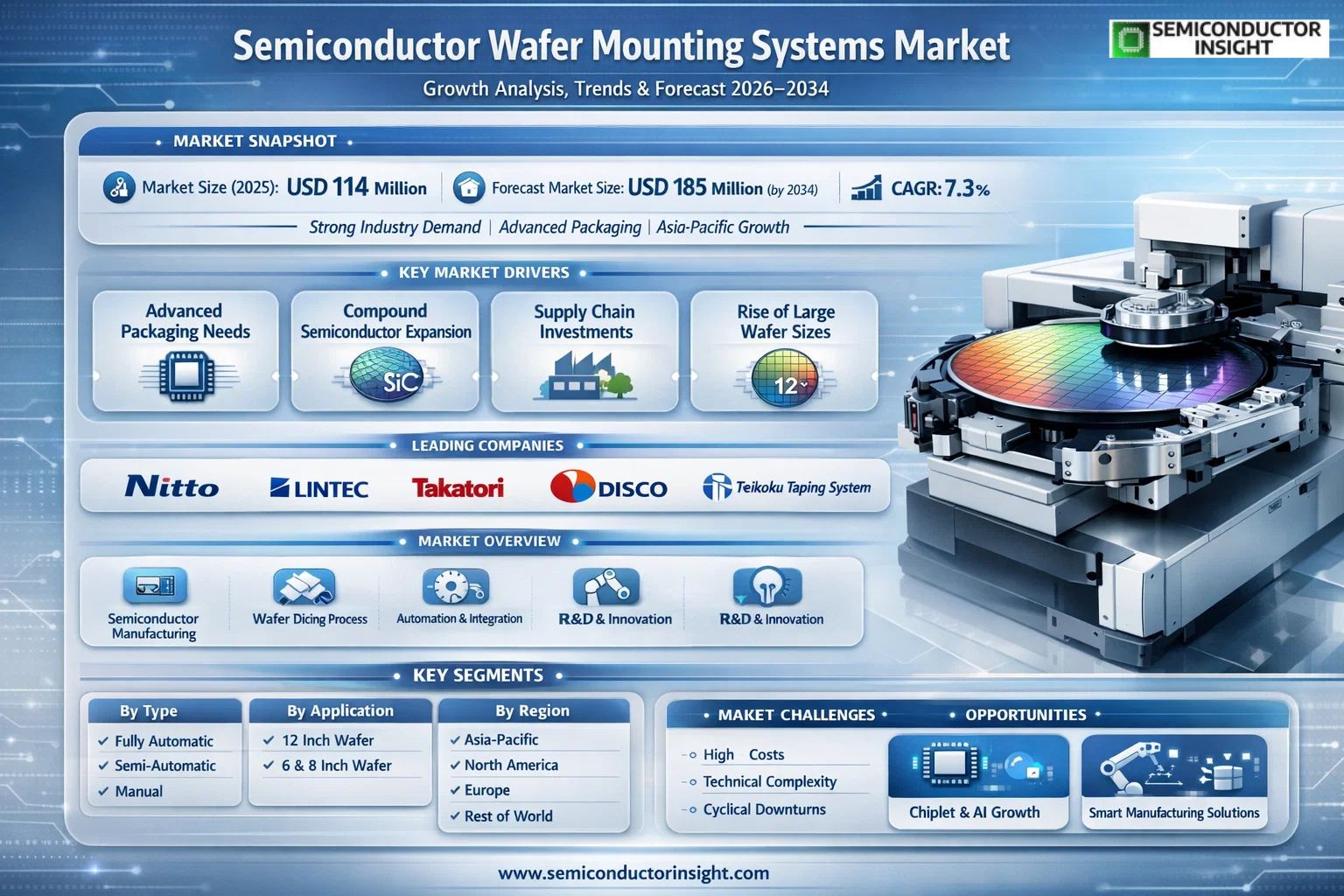
Global Semiconductor Wafer Mounting Systems market size was valued at USD 114 million in 2025. The market is projected to grow from USD 122.4 million in 2026 to USD 185 million by 2034, exhibiting a CAGR of 7.3% during the forecast period.
Semiconductor wafer mounting systems are specialized equipment used in the back-end semiconductor manufacturing process. These systems perform the critical step of mounting a thinned wafer onto a dicing tape or film that is stretched across a metal frame, a process essential for protecting the wafer during subsequent dicing and handling. This step is vital because it reduces particulate contamination and prevents damage, thereby ensuring high yields and reliable performance of the final semiconductor devices. The equipment can be categorized into fully automatic, semi-automatic, and manual types, with automation driving efficiency in high-volume production environments.
The market’s growth is intrinsically linked to the expansion of the broader semiconductor industry. For instance, WSTS has projected strong growth for Global semiconductor market, forecasting it to reach USD 611 billion in 2025 and further grow to USD 687 billion by 2026. This robust expansion, particularly in segments like Memory and Logic which are expected to see increases of over 25% and 10% respectively in 2026, directly fuels demand for advanced backend equipment like wafer mounters. Furthermore, regional manufacturing hubs in Asia Pacific and the Americas are experiencing significant investment, creating a favorable environment for equipment suppliers. Key players such as Nitto Denko, LINTEC Corporation, DISCO Corporation, and Takatori Corporation dominate this specialized market from their stronghold in Japan.
MARKET DRIVERS
Persistent Demand from Advanced Packaging
The relentless innovation in advanced semiconductor packaging technologies, such as 2.5D/3D chip integration and fan-out wafer-level packaging (FOWLP), is a primary driver for the Semiconductor Wafer Mounting Systems Market. These complex packaging schemes require exceptionally precise and reliable wafer handling and bonding during the temporary mounting process onto carrier substrates. As semiconductor device manufacturers push for greater performance in smaller form factors, the demand for sophisticated mounting systems that offer superior control over warpage, stress, and alignment continues to accelerate, supporting market growth of over 7% annually.
Expansion of Compound Semiconductor Fabrication
The proliferation of devices based on gallium nitride (GaN) and silicon carbide (SiC) for power electronics and RF applications necessitates specialized handling. These compound semiconductor wafers are often thinner and more brittle than traditional silicon, creating a critical need for mounting systems engineered to manage their unique material properties. This expansion into new substrate materials directly fuels investments in next-generation wafer mounting equipment designed for higher throughput and reduced breakage.
➤ Industry analysis consistently finds that leading-edge packaging fabs now allocate a significant portion of their capital equipment budget to advanced wafer-level processing tools, including precision mounting systems.
Furthermore, Global push for semiconductor supply chain resilience and new fab construction, particularly for mature and specialty nodes, generates steady demand for reliable, high-throughput wafer mounting systems as foundational tools in the assembly and packaging line.
MARKET CHALLENGES
Technical Complexity and Process Integration
A core challenge in the Semiconductor Wafer Mounting Systems Market is managing the intricate technical requirements of new heterogeneous integration workflows. Process engineers must balance parameters like adhesive thickness, curing temperature, and debonding force without inducing thermal stress or contamination. Integrating the mounting system seamlessly into fully automated lines with other equipment for thinning, inspection, and dicing requires significant customization and software development, increasing total cost of ownership and complicating deployment.
Other Challenges
Adhesive Material Limitations
The performance of temporary bonding adhesives, which are integral to the mounting process, presents a bottleneck. Developing adhesives that can withstand subsequent high-temperature processes yet allow for clean, residue-free debonding remains a persistent hurdle, directly impacting yield and throughput for system manufacturers.
Cost Sensitivity in Mature Segments
While advanced packaging drives premium system sales, price pressure is intense in markets for more mature semiconductor devices. Manufacturers in these segments often prioritize cost over cutting-edge performance, challenging equipment suppliers to offer reliable yet economically viable solutions for the broader Semiconductor Wafer Mounting Systems Market.
MARKET RESTRAINTS
High Capital Investment and Cyclical Industry Downturns
Primary restraint on the Semiconductor Wafer Mounting Systems Market is the substantial capital expenditure required for this highly specialized equipment. A single advanced system can cost several million dollars, creating a significant barrier for smaller packaging and assembly houses. Furthermore, the inherent cyclicality of the semiconductor industry leads to periods of reduced capital spending by chipmakers. During these downturns, investments in new assembly and packaging tools, including wafer mounting systems, are often deferred or scaled back, directly impacting equipment manufacturers’ order volumes and revenue streams.
MARKET OPPORTUNITIES
Growth of Chiplet-Based Architectures and AI Hardware
The rapid adoption of chiplet-based designs and specialized AI accelerators represents a major opportunity. These architectures involve assembling multiple known-good dies (KGD) onto an interposer or substrate, a process heavily reliant on precision wafer-level temporary bonding and thinning. This trend necessitates mounting systems capable of handling ultra-thin wafers and diverse die sizes with nanometer-level accuracy, creating a new, high-value segment for innovative equipment vendors in the Semiconductor Wafer Mounting Systems Market.
Adoption of Advanced Process Control and Smart Manufacturing
Integrating advanced sensors, in-line metrology, and AI-driven process control directly into wafer mounting systems presents a significant value-adding opportunity. Equipment that can provide real-time data on bond quality, thickness variation, and stress distribution enables predictive maintenance and closed-loop process optimization. This shift towards smart, Industry 4.0-ready tools can command premium pricing and foster stronger long-term partnerships with large-scale semiconductor manufacturers focused on yield maximization.
Key Semiconductor Wafer Mounting Systems Market Trends
Automation and Integration for Advanced Wafer Processing
The industry is undergoing a significant shift towards fully automated wafer mounting solutions. This trend is driven by the need for higher throughput, improved yield, and reduced particulate contamination in cleanroom environments. As semiconductor devices become more complex and wafer sizes standardize around 12-inch formats, manufacturers are integrating mounting systems more seamlessly into smart fab lines. This push for automation supports the broader industry growth projected by WSTS, particularly in the Logic and Memory segments which require highly efficient backend processing to meet soaring demand.
Other Trends
Expansion of Production Capacity in Asia Pacific
Leading manufacturers, predominantly based in Japan, are expanding their operational footprint and supplier networks across the Asia Pacific region. This geographic trend aligns with WSTS forecasts indicating this region as a primary growth engine for the overall semiconductor market. The concentration of new fab construction in countries like Taiwan, South Korea, and China is creating sustained demand for advanced wafer mounting equipment, prompting global players to strengthen their local presence for sales and service.
Material and Process Innovation
Innovation is focused on the tapes and films used in the mounting process, with suppliers developing advanced adhesive materials that offer superior performance during subsequent grinding and dicing steps. This evolution is critical for handling thinner and more fragile wafers. The competitive landscape includes specialized players like Nitto Denko and LINTEC Corporation, who are key drivers of this material science trend. Concurrently, equipment is being designed for greater flexibility to handle multi-generational wafer sizes, including 6, 8, and 12-inch wafers, as the market transitions.
COMPETITIVE LANDSCAPE
Key Industry Players
A Consolidated Market Led by Japanese Precision Engineering
Global Semiconductor Wafer Mounting Systems market is characterized by a high degree of consolidation, with Japanese manufacturers dominating the competitive landscape through technological excellence and deep integration within the semiconductor supply chain. Leading this segment is Nitto Denko, a global specialty materials giant, which commands a significant market share. Its strength lies in providing comprehensive solutions that pair advanced mounting tapes with highly reliable automated mounting equipment. Close competitors such as LINTEC Corporation and DISCO Corporation reinforce Japan’s stronghold; LINTEC leverages its adhesive tape expertise, while DISCO’s prowess in precision cutting tools creates synergies for integrated back-end process solutions. This core group sets high standards for precision, throughput, and process integration, particularly for high-volume 12-inch wafer fabrication, making the market entry barrier substantial for new players.
Beyond the dominant Japanese leaders, several significant niche and regional players contribute to a diversified competitive environment. Companies like Teikoku Taping System and Takatori Corporation offer specialized and highly automated systems, catering to specific process requirements. In South Korea, CUON Solution has emerged as a key supplier, indicating the market’s expansion within major semiconductor manufacturing clusters. Meanwhile, players such as Technovision, Advanced Dicing Technologies (ADT), and Ultron Systems Inc. focus on innovations for advanced packaging, heterogeneous integration, and the growing demand for 6-inch and 8-inch wafer refurbishment and MEMS production. The competitive dynamic is further shaped by regional suppliers in China, including Jiangsu Jcxj and Heyan Technology, which are increasingly serving domestic fabs, adding a layer of regional competition based on cost-effectiveness and local support.
List of Key Semiconductor Wafer Mounting Systems Companies Profiled
- Nitto Denko
- LINTEC Corporation
- Takatori Corporation
- DISCO Corporation
- Teikoku Taping System
- NPMT (NDS)
- Technovision
- Dynatech Co.,Ltd
- CUON Solution
- Ultron Systems Inc
- Semiconductor Equipment Corporation
- AE Advanced Engineering
- Powatec
- Advanced Dicing Technologies (ADT)
- Heyan Technology
Segment Analysis:
| Segment Category | Sub-Segments | Key Insights |
| By Type |
|
Fully Automatic Wafer Mounting Machines are the leading segment, driven by the semiconductor industry’s relentless push for higher throughput and precision in advanced fabrication.
|
| By Application |
|
12 Inch Wafer applications dominate the market demand, as this size is the standard for leading-edge logic and memory chip production where cost-per-die efficiency is paramount.
|
| By End User |
|
Foundries represent the most critical and demanding end-user segment, acting as the primary growth engine for high-performance mounting systems.
|
| By Automation Level Integration |
|
Cluster Tool Integrated Modules are emerging as the leading strategic trend, moving beyond mere automation to seamless process integration.
|
| By Process Criticality |
|
Ultra-Thin & Fragile Wafer Mounting is the highest-value and most technologically demanding segment, driven by the needs of 3D integration and advanced mobility devices.
|
Regional Analysis: Semiconductor Wafer Mounting Systems Market
Asia-Pacific
Taiwan and South Korea form the technological core of the market. Home to leading foundries and memory manufacturers, these countries demand the most advanced wafer mounting systems for high-volume production of leading-edge nodes. The continuous cycle of fab upgrades and capacity expansion to support advanced packaging like chip-on-wafer-on-substrate (CoWoS) ensures a consistent, high-value demand flow for precision mounting equipment from top-tier suppliers.
China’s market dynamics are shaped by a national strategic push for semiconductor independence, leading to unprecedented investment in domestic fabrication capacity. This creates a dual demand stream: for cutting-edge systems in new flagship fabs and for reliable, cost-effective mounting solutions in the vast ecosystem of smaller packaging houses. This environment fosters both competition and partnership between international vendors and emerging local equipment makers.
Japan maintains a strong position through its expertise in materials, sensors, and power devices, requiring highly reliable and precise mounting systems for these specialized applications. Meanwhile, Southeast Asian nations, particularly Malaysia and Singapore, are key hubs for OSAT activities, generating steady demand for robust, high-uptime wafer mounting systems that cater to a wide variety of packaging types and customer requirements.
The region’s leadership is reinforced by a deeply integrated supply chain. Proximity to wafer and substrate suppliers, adhesive manufacturers, and tool integrators allows for rapid co-development of next-generation mounting processes. This ecosystem enables equipment vendors to iterate quickly based on direct feedback from leading-edge fabs, accelerating innovation cycles for wafer-level packaging and heterogeneous integration solutions.
North America
North America, led by the United States, is a vital innovation and demand center for advanced Semiconductor Wafer Mounting Systems, particularly for R&D, low-volume/high-mix production, and cutting-edge packaging research. The market is fueled by leading fabless semiconductor companies, integrated device manufacturers (IDMs), and premier research institutions that pioneer next-generation architectures like 3D integration and chiplets. Demand is characterized by a need for highly flexible, programmable mounting systems that can handle experimental processes, novel materials, and diverse substrate types. The focus on regaining domestic manufacturing capability through acts like the CHIPS and Science Act is beginning to stimulate new investments in advanced packaging facilities, which will require state-of-the-art wafer mounting and bonding equipment, positioning the region for future growth in high-value system segments.
Europe
The European market for Semiconductor Wafer Mounting Systems is defined by specialization and high-value manufacturing. The regional demand is strongest in automotive, industrial, and security applications, where reliability and precision for technologies like power semiconductors, MEMS, and sensors are paramount. Key automotive hubs in Germany, along with significant semiconductor clusters in regions like Dresden (Germany) and Grenoble (France), drive demand for robust mounting solutions capable of meeting stringent automotive-grade quality standards. The European strategy, exemplified by the European Chips Act, focuses on bolstering sovereignty in specific semiconductor technologies, which will increase investment in niche manufacturing capabilities and subsequently in the specialized back-end equipment, including mounting systems, needed to support them.
South America
The Semiconductor Wafer Mounting Systems Market in South America is nascent but developing, primarily serving regional electronics assembly and niche industrial applications. Brazil is the most significant market, with demand stemming from local consumer electronics production and the automotive sector. The region largely relies on imports of established, cost-effective mounting equipment rather than cutting-edge systems, focusing on reliability and maintenance support for existing production lines. Growth is gradual and tied to broader industrial development and stability. Regional dynamics involve occasional government incentives for local electronics manufacturing, which can spur incremental investments in semiconductor packaging infrastructure and the associated wafer mounting tools required for basic assembly operations.
Middle East & Africa
The market for Semiconductor Wafer Mounting Systems in the Middle East & Africa region is currently minimal but holds long-term strategic potential. Activity is largely concentrated in a few technology hubs, such as in Israel for specialized semiconductor design and in the UAE for strategic technology investments. The primary market dynamic is not yet centered on high-volume fabrication but on establishing initial capabilities and attracting knowledge. Any near-term demand for mounting systems would likely be for R&D, pilot lines, or educational purposes within new technology institutes and partnerships. Future growth is contingent on major, sustained investments in semiconductor manufacturing ecosystems, which remain in early planning stages compared to other global regions.
Report Scope
This market research report provides a comprehensive analysis of the Semiconductor Wafer Mounting Systems Market , covering the forecast period 2026–2034. It offers detailed insights into market dynamics, technological advancements, competitive landscape, and key trends shaping the industry.
Key focus areas of the report include:
- Market Overview: The report begins with an overview outlining the market’s current scenario, key growth indicators, and industry transformation drivers. It discusses macroeconomic factors, demand–supply balance, regulatory landscape, and the strategic role of wafer mounting in the semiconductor fabrication process for reducing contamination and ensuring device efficiency across industries such as computing, consumer electronics, automotive, and telecommunications.
- Market Size & Forecast: Historical data and future projections for revenue, unit shipments, and market value across major regions and segments, with a forecasted CAGR of 7.3%.
- Segmentation Analysis: Detailed breakdown by product type (Fully Automatic, Semi-automatic, Manual Wafer Mounting Machines), application (12 Inch, 6 & 8 Inch Wafers), and end-user industry to identify high-growth segments and investment opportunities.
- Regional Insights: Insights into market performance across North America, Europe, Asia-Pacific, South America, and the Middle East & Africa, including country-level analysis for major economies.
- Competitive Landscape: Profiles of leading market participants, including their product offerings, manufacturing capacity, market share, pricing strategies, and recent developments such as mergers, acquisitions, and partnerships.
- Technology Trends & Innovation: Assessment of emerging technologies, automation trends in wafer mounting, fabrication techniques, and evolving industry standards influenced by the broader semiconductor market growth.
- Market Drivers & Restraints: Evaluation of factors driving market growth along with challenges, supply chain constraints, regulatory issues, and market-entry barriers.
- Stakeholder Insights: Insights for equipment manufacturers, semiconductor foundries, component suppliers, investors, and policymakers regarding the evolving ecosystem and strategic opportunities.
Primary and secondary research methods are employed, including interviews with industry experts, surveys of manufacturers and suppliers, data from verified sources, and real-time market intelligence to ensure the accuracy and reliability of the insights presented.
FREQUENTLY ASKED QUESTIONS:
What is the current market size of Semiconductor Wafer Mounting Systems Market?
-> Global Semiconductor Wafer Mounting Systems Market was valued at USD 114 million in 2025 and is projected to reach USD 185 million by 2034, growing at a CAGR of 7.3% during the forecast period.
Which key companies operate in Semiconductor Wafer Mounting Systems Market?
-> Key players include Nitto Denko, LINTEC Corporation, Takatori Corporation, DISCO Corporation, Teikoku Taping System, NPMT (NDS), Technovision, Dynatech Co.,Ltd, CUON Solution, and Ultron Systems Inc, among others. Many key manufacturers are based in Japan.
What are the key growth drivers?
-> Key growth drivers include the overall expansion of Global semiconductor market, particularly in Logic and Memory segments; strong projected growth in semiconductor end-markets like computing; significant regional investments and growth in the Americas and Asia Pacific; and the essential role of wafer mounting in reducing particulate contamination for efficient device fabrication.
Which region dominates the market?
-> Asia is a key region, with major manufacturers based in Japan. The Americas and Asia Pacific are projected to see significant semiconductor market growth, which drives demand for wafer mounting systems.
What are the emerging trends?
-> Emerging trends include increased automation in wafer mounting processes, growth driven by large wafer sizes (12 Inch), integration with advanced dicing and fabrication lines, and technology advancements fueled by the broader semiconductor industry’s push towards higher efficiency and performance.

Get Sample Report PDF for Exclusive Insights
Report Sample Includes
- Table of Contents
- List of Tables & Figures
- Charts, Research Methodology, and more...
 Download Sample Report PDF