
Semiconductor Photomask Inspection Equipment Market Insights
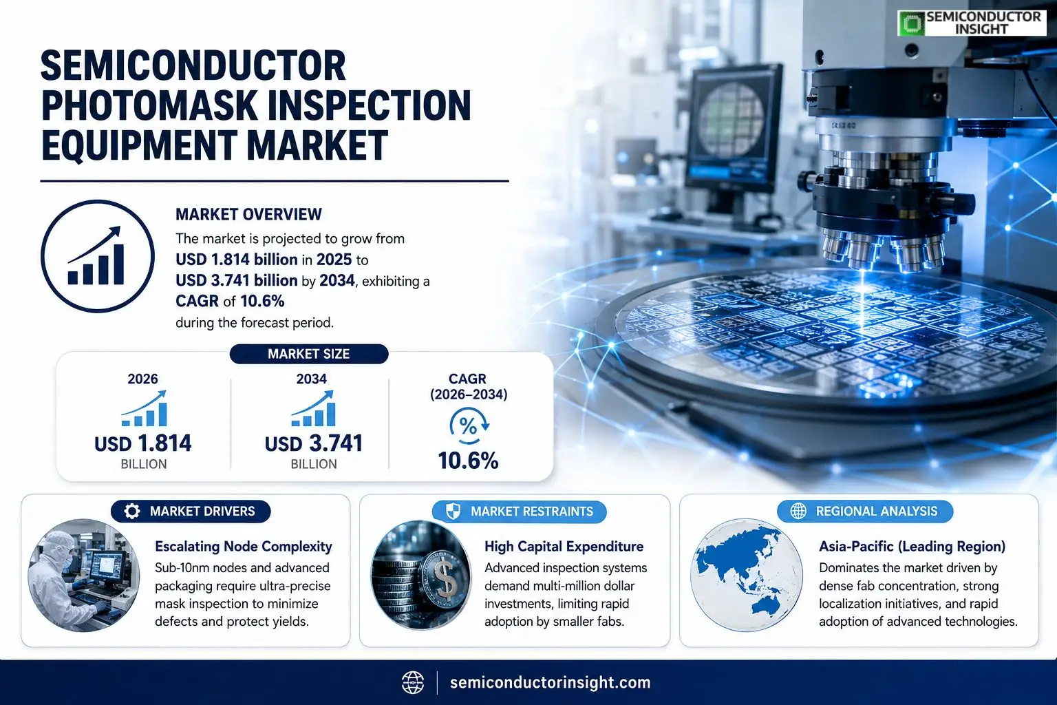
Semiconductor Photomask Inspection Equipment market size was valued at USD 1.814 billion in 2025. Forecasts indicate growth to USD 3.741 billion by 2034, reflecting a compound annual growth rate of 10.6 % over the period.
The equipment suite comprises high‑resolution detection systems and substrate testing units that verify photomasks before lithography steps. A photomask serves as the master pattern for transferring integrated‑circuit designs onto silicon wafers; any defect larger than the process window can compromise yield. Inspection tools therefore combine optical microscopy, electron‑beam imaging and advanced algorithms to locate sub‑nanometer anomalies and certify mask integrity.Market momentum stems from several converging forces. The surge in sub‑7 nm AI compute chips and ultra‑high‑definition display panels raises demand for ultra‑precise mask inspection capability. Simultaneously, the rollout of high‑NA EUV lithography introduces curved‑mask formats that require next‑generation sensors and software. In the Asia‑Pacific regionparticularly Chinapolicy incentives accelerate domestic sourcing of inspection hardware, reshaping the competitive landscape. Finally, artificial‑intelligence analytics are being embedded into defect classification workflows, while automation drives end‑to‑end inspection lines that reduce cycle time and human error.
MARKET DRIVERS
Escalating Node Complexity
The shift toward sub‑10‑nanometer logic nodes compels wafer fabs to demand tighter pattern fidelity. As feature dimensions shrink, even minute mask defects can propagate costly yield losses, prompting manufacturers to upgrade to higher‑resolution inspection platforms. The Semiconductor Photomask Inspection Equipment Market therefore experiences a surge in orders from leading foundries seeking to safeguard process windows.
Regulatory and Quality Standards
International standards such as IEC 61331 and emerging EU safety guidelines impose stringent defect‑density thresholds. Compliance pressures drive fabs to adopt inspection tools with advanced defect classification algorithms, accelerating capital investment cycles. Companies that integrate AI‑enhanced defect detection are gaining a competitive edge as customers prioritize traceability.
➤ “Investors are allocating capital to photomask inspection firms that can demonstrate a 30 % reduction in false‑positive rates, unlocking significant cost savings for chip makers.”
Beyond technology, the expansion of advanced packagingespecially fan‑out wafer‑level packagingcreates new inspection checkpoints. As more layers are stacked, mask integrity becomes critical for multi‑chip modules, reinforcing the strategic importance of sophisticated inspection solutions within the Semiconductor Photomask Inspection Equipment Market.
MARKET CHALLENGES
High Capital Expenditure
State‑of‑the‑art inspection systems command multi‑million dollar price tags, which can strain the capital budgets of smaller fabs and research labs. The financial outlay is justified by long‑term yield improvements, yet the upfront cost creates a barrier to rapid adoption, especially in regions where fab construction is still emerging.
Other Challenges
Skill Shortage
Operating next‑generation inspection equipment requires expertise in optics, data analytics, and machine learning. The talent pool remains limited, forcing companies to invest in extensive training programs or partner with specialist service providers, which can delay deployment timelines.
MARKET RESTRAINTS
Supply‑Chain Volatility
Periodic shortages of high‑purity optical components and precision mechanical sub‑assemblies have disrupted production schedules for inspection system manufacturers. When lead times extend, customers often defer upgrades, dampening short‑term growth momentum for the Semiconductor Photomask Inspection Equipment Market.
MARKET OPPORTUNITIES
Integration of Predictive Analytics
Embedding predictive maintenance and defect‑forecasting models into inspection workflows can transform equipment from a passive quality gate into a proactive yield‑optimization tool. Vendors that package these capabilities as software‑as‑a‑service stand to capture recurring revenue streams while delivering measurable cost reductions to end users, opening a lucrative avenue for market expansion.
Semiconductor Photomask Inspection Equipment Market Trends
Demand for High‑Resolution Masks Driven by AI Chip and Display Markets
The surge in AI‑compute chip orders and the push for 4K/8K display panels are pressuring mask makers to adopt inspection tools that resolve sub‑10‑nanometer defects. Unlike earlier generations, today’s photomasks must guarantee pattern fidelity across multi‑chip modules, a requirement that amplifies the need for equipment capable of high‑resolution imaging and rapid defect classification. Vendors that integrate advanced optics with real‑time data analytics are seeing stronger purchase intent from fab lines that cannot afford yield losses. Consequently, the Semiconductor Photomask Inspection Equipment Market is reshaping its product roadmap toward higher numerical‑aperture systems and tighter throughput specifications. Operators are also redefining maintenance schedules to align with the continuous‑run models adopted by AI server manufacturers, shortening time‑to‑market and turning equipment performance into a strategic lever for semiconductor fabs.
Other Trends
Technological Iteration: From EUV to Curved Masks
The transition from traditional flat masks to curvature‑compensated designs reflects lithography’s march toward higher resolution. High‑NA EUV tools demand mask surfaces that conform to non‑planar geometries, prompting inspection suppliers to develop metrology heads that can interrogate both flat and curved substrates without sacrificing sensitivity. In parallel, algorithms powered by machine learning are being embedded directly into inspection hardware to differentiate between process‑induced anomalies and benign pattern variations. This dual focus on mechanical adaptability and intelligent defect discrimination reduces false‑positive rates and shortens engineer review cycles. As a result, manufacturers are able to certify new mask formats more rapidly, reinforcing the competitive edge of early adopters in the Semiconductor Photomask Inspection Equipment Market.
Regional Localization Accelerates in Asia‑Pacific
Asia‑Pacific remains the dominant consumption hub, yet geopolitical pressures are accelerating domestic sourcing of inspection platforms, especially in China. Policy incentives and subsidies are encouraging local equipment firms to bridge technology gaps through joint ventures with established players. The emerging supply chain for domestically produced inspection units shortens lead times and diminishes reliance on imported spare parts, a factor that resonated with several large fab operators during recent capacity expansions. While the region continues to command the largest share of procurement, the shift toward localized manufacturing is redefining the competitive landscape for the Semiconductor Photomask Inspection Equipment Market, presenting opportunities for vendors that can align their roadmaps with regional standards and regulatory expectations.
COMPETITIVE LANDSCAPEKey Industry Players
Competitive Dynamics in the Photomask Inspection Equipment Market
The market is anchored by a handful of large‐scale manufacturers whose product portfolios span the full spectrum of detection, substrate testing, and AI‑enhanced analysis. KLA Corp. remains the de‑facto leader, leveraging its deep expertise in defect inspection and a robust service network that gives it a decisive edge in high‑volume semiconductor fabs. Its machines command premium pricing, yet the breadth of its offeringfrom conventional optical systems to emerging high‑NA EUV solutionscreates a barrier to entry for smaller rivals. The concentration around KLA has prompted a tiered structure: top‑tier OEMs dominate the $4 billion segment, while mid‑tier players compete on specialized capabilities such as curved‑mask inspection or rapid‑turnaround services.Beyond the dominant tier, a constellation of niche innovators is shaping the market’s forward momentum. Applied Materials and Lasertec supply complementary platforms that excel in throughput for mid‑range nodes, while Japan‑based NuFlare and Advantest focus on precision tools for sub‑7 nm processes. European heavyweight Carl Zeiss contributes advanced optics, and Chinese entrant Visionoptech is rapidly expanding its domestic footprint through government‑backed programs. Additional playersincluding Tokyo Electron, ASML (through its mask‑related metrology unit), Nanometrics, and Samsung Techwintarget specific application niches such as AI‑driven defect classification or fully automated inspection lines. Their collective activity injects diversity into the supply chain and offers fabs alternative avenues for technology adoption.
List of Key Semiconductor Photomask Inspection Equipment Companies Profiled
- KLA Corp.
- Applied Materials
- Lasertec Corp.
- NuFlare
- Carl Zeiss AG
- Advantest
- Visionoptech
- Tokyo Electron Ltd.
- ASML Holding NV
- Nanometrics Inc.
- Samsung Techwin
- Cymer (a division of ASML)
- VDM Systems
Segment Analysis:
| Segment Category | Sub-Segments | Key Insights |
| By Type |
|
Photomask Detection Equipment
|
| By Application |
|
Semiconductor Chip Manufacturer
|
| By End User |
|
Fabrication Facilities
|
| By Technology Trend |
|
AI‑Driven Inspection
|
| By Market Driver |
|
AI Chip Boom
|
Regional Analysis: Semiconductor Photomask Inspection Equipment Market
Asia‑Pacific
Asian fabs are integrating machine‑learning‑enhanced inspection platforms at a speed that outstrips other regions, driven by the need to maintain yield in leading‑edge nodes. Vendors that bundle predictive analytics with hardware see higher adoption rates.
Proximity to mask‑making fabs and lithography equipment makers creates a virtuous loop where feedback on defect profiles quickly informs inspection tool upgrades, shortening development timelines.
Governmental chip subsidies and tax incentives have softened the financial hurdle for acquiring next‑generation inspection gear, prompting mid‑size fabs to transition from legacy systems.
A dense pool of photomask specialists and academic research centers fuels continuous innovation, ensuring that equipment vendors can co‑develop bespoke solutions for demanding process nodes.
North America
North America remains a strong secondary market, anchored by a mature ecosystem of semiconductor design houses and R&D facilities. The region’s emphasis on advanced packaging and 3‑D integration compels fabs to adopt inspection tools with heightened sensitivity to overlay and line‑edge roughness. While overall equipment volumes trail Asia‑Pacific, the market is characterized by a willingness to pay a premium for fully integrated metrology suites that combine inspection with pattern‑matching capabilities. Strategic partnerships between equipment manufacturers and leading academic institutions foster a pipeline of proprietary algorithms, reinforcing the region’s reputation for high‑value, differentiated solutions.
Europe
Europe’s Semiconductor Photomask Inspection Equipment Market is shaped by a consortium‑driven approach, where cross‑border initiatives fund joint development projects. The emphasis on sustainability and energy‑efficient tooling influences purchasing decisions, prompting operators to favor platforms with low power draw and modular designs. Although the European fab base is smaller, it focuses on specialty nodes such as analog and RF, which demand inspection equipment capable of handling diverse mask designs. This niche focus drives vendors to tailor software suites for mixed‑signal environments, creating a distinct value proposition within the continent.
South America
South America’s engagement with the Semiconductor Photomask Inspection Equipment Market is still embryonic, yet growing pockets of assembly and test facilities are beginning to recognize the cost‑benefit of in‑line inspection. Local manufacturers are increasingly outsourcing mask production to Asian partners, but the desire to reduce turnaround times has sparked interest in compact, cost‑effective inspection stations. Governments are introducing modest incentives to attract semiconductor investments, which could translate into a gradual rise in demand for entry‑level inspection solutions that balance performance with affordability.
Middle East & Africa
The Middle East & Africa region exhibits a cautious but optimistic outlook for the Semiconductor Photomask Inspection Equipment Market. Emerging smart‑city and IoT initiatives are prompting governments to explore semiconductor fabrication as part of diversification strategies. While the current footprint is limited to pilot lines and research labs, the region’s emphasis on technology transfer agreements suggests a future appetite for inspection equipment that can be integrated into nascent fabs. Partnerships with established Asian vendors are anticipated to accelerate capability building, positioning the region for a modest yet strategic entry into the market.
Report Scope
This market research report provides a comprehensive analysis of the Semiconductor Photomask Inspection Equipment Market , covering the forecast period 2026–2034. It offers detailed insights into market dynamics, technological advancements, competitive landscape, and key trends shaping the industry.
Key focus areas of the report include:
- Market Overview: The report begins with an overview outlining its current market scenario, key growth indicators, and industry transformation drivers. It discusses macroeconomic factors, demand–supply balance, regulatory landscape, and the strategic role of semiconductors in powering advancements across industries such as automotive, telecommunications, consumer electronics, and industrial automation.
- Market Size & Forecast: Historical data and future projections for revenue, unit shipments, and market value across major regions and segments.
- Segmentation Analysis: Detailed breakdown by product type, technology, application, and end-user industry to identify high-growth segments and investment opportunities.
- Regional Insights: Insights into market performance across North America, Europe, Asia-Pacific, Latin America, and the Middle East & Africa, including country-level analysis where relevant.
- Competitive Landscape: Profiles of leading market participants, including their product offerings, R&D focus, manufacturing capacity, pricing strategies, and recent developments such as mergers, acquisitions, and partnerships.
- Technology Trends & Innovation: Assessment of emerging technologies, integration of AI/IoT, semiconductor design trends, fabrication techniques, and evolving industry standards.
- Market Drivers & Restraints: Evaluation of factors driving market growth along with challenges, supply chain constraints, regulatory issues, and market-entry barriers.
- Stakeholder Insights: Insights for component suppliers, OEMs, system integrators, investors, and policymakers regarding the evolving ecosystem and strategic opportunities.
Primary and secondary research methods are employed, including interviews with industry experts, data from verified sources, and real-time market intelligence to ensure the accuracy and reliability of the insights presented.
FREQUENTLY ASKED QUESTIONS:
What is the current market size of Semiconductor Photomask Inspection Equipment Market?
-> Semiconductor Photomask Inspection Equipment Market was valued at USD 1,814 million in 2025 and is expected to reach USD 3,741 million by 2034, growing at a CAGR of 10.6%.
Which key companies operate in Semiconductor Photomask Inspection Equipment Market?
-> Key players include KLA (US), Applied Materials (US), Lasertec (JP), NuFlare (JP), Carl Zeiss AG (DE), Advantest (JP) and Visionoptech (CN).
What are the key growth drivers?
-> Key growth drivers include explosive demand for sub‑7nm AI compute chips, high‑resolution 4K/8K display masks, advancement of high‑NA EUV and curved mask technologies, and increasing AI‑enabled inspection automation.
Which region dominates the market?
-> Asia-Pacific remains the largest consumer market, with China leading localization efforts and driving rapid growth.
What are the emerging trends?
-> Emerging trends include integration of AI for defect discrimination, full‑process automation, development of high‑NA EUV inspection solutions, and the shift toward curved mask inspection platforms.

Get Sample Report PDF for Exclusive Insights
Report Sample Includes
- Table of Contents
- List of Tables & Figures
- Charts, Research Methodology, and more...






