Market Insights
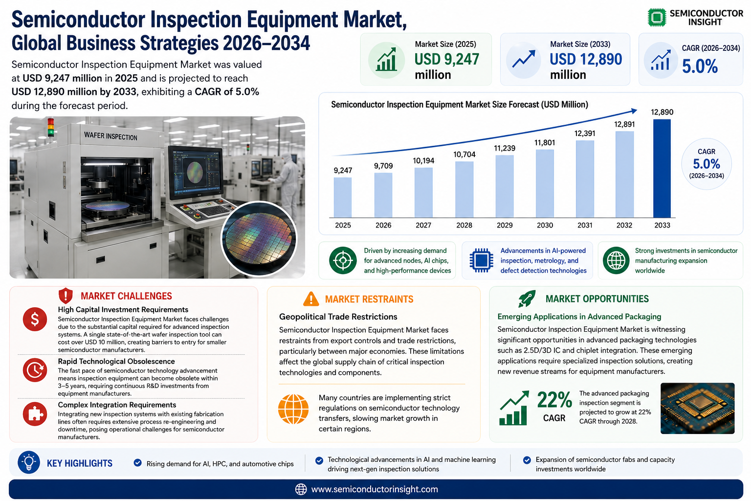
Global Semiconductor Inspection Equipment Market was valued at USD 9,247 million in 2025 and is projected to reach USD 12,890 million by 2033, exhibiting a CAGR of 5.0% during the forecast period.
Semiconductor Inspection Equipment Market plays a critical role in ensuring the quality and reliability of semiconductor manufacturing processes. These systems detect defects, measure critical dimensions, and verify alignment across multiple stages of wafer fabrication. Key segments include defect inspection equipment, metrology tools, optical inspection systems, and wafer-level testing solutions. With semiconductor manufacturing involving 400 to 600 intricate steps over one to two months per wafer batch, even minor defects can lead to significant yield losses making inspection technologies indispensable for cost control and performance optimization.
The market growth is driven by increasing demand for advanced chips in AI, IoT, and automotive applications alongside shrinking transistor geometries that require nanometer-level precision. Asia-Pacific dominates with over 77% market share due to concentrated foundry capacity in Taiwan and South Korea. KLA Corporation leads the competitive landscape with >30% market share through its comprehensive portfolio of process control solutions. Recent technological advancements include AI-powered defect classification and hyperspectral imaging for sub-3nm node development.
MARKET DRIVERS
Growing Demand for Miniaturized Semiconductor Components
Semiconductor Inspection Equipment Market is driven by the increasing demand for smaller, more powerful chips in consumer electronics and automotive applications. Manufacturers are investing heavily in advanced inspection tools to detect nanoscale defects in increasingly complex semiconductor designs. The global push toward 5G technology has further accelerated this need for precision inspection solutions.
Automation in Semiconductor Fabrication
As semiconductor fabs transition to Industry 4.0 standards, automated inspection systems are becoming crucial for maintaining production efficiency. The adoption of AI-powered inspection equipment has grown by over 35% in the past three years, enabling real-time defect detection and classification. This automation trend is significantly boosting market growth.
Stringent quality requirements in critical industries such as aerospace and medical devices are also propelling demand for high-accuracy inspection systems. Manufacturers cannot afford defects in these sensitive applications, creating sustained demand for advanced inspection technologies.
MARKET CHALLENGES
High Capital Investment Requirements
Semiconductor Inspection Equipment Market faces challenges due to the substantial capital required for advanced inspection systems. A single state-of-the-art wafer inspection tool can cost over USD 10 million, creating barriers to entry for smaller semiconductor manufacturers.
Other Challenges
Rapid Technological Obsolescence
The fast pace of semiconductor technology advancement means inspection equipment can become obsolete within 3-5 years, requiring continuous R&D investments from equipment manufacturers.
Complex Integration Requirements
Integrating new inspection systems with existing fabrication lines often requires extensive process re-engineering and downtime, posing operational challenges for semiconductor manufacturers.
MARKET RESTRAINTS
Geopolitical Trade Restrictions
Semiconductor Inspection Equipment Market faces restraints from export controls and trade restrictions, particularly between major economies. These limitations affect the global supply chain of critical inspection technologies and components. Many countries are implementing strict regulations on semiconductor technology transfers, slowing market growth in certain regions.
MARKET OPPORTUNITIES
Emerging Applications in Advanced Packaging
Semiconductor Inspection Equipment Market is witnessing significant opportunities in advanced packaging technologies such as 2.5D/3D IC and chiplet integration. These emerging applications require specialized inspection solutions, creating new revenue streams for equipment manufacturers. The advanced packaging inspection segment is projected to grow at 22% CAGR through 2028.
Expansion of Domestic Semiconductor Production
Government initiatives worldwide to establish domestic semiconductor capabilities are creating substantial opportunities for inspection equipment providers. Nearly USD 200 billion in subsidies and incentives have been announced globally to boost local semiconductor production, directly benefiting the inspection equipment market.
Semiconductor Inspection Equipment Market Trends
Rising Demand for Advanced Inspection Solutions
Semiconductor Inspection Equipment Market is experiencing steady growth, projected to reach USD 12.89 billion by 2033 with a 5.0% CAGR. This growth is driven by increasing complexity in semiconductor manufacturing, where up to 600 process steps require precise defect detection. The Asia-Pacific region dominates the market with over 77% share, primarily due to concentrated semiconductor production facilities in countries like China, South Korea, and Taiwan.
Other Trends
Defect Inspection Dominates Equipment Segments
Defect inspection equipment holds over 55% market share, critical for maintaining yield rates in wafer production. Optical and macro defect inspection systems are gaining adoption as node sizes shrink below 7nm, requiring more sensitive detection capabilities. Leading manufacturers are integrating AI-driven pattern recognition to improve defect classification accuracy.
Emerging Technological Advancements
The market is seeing rapid innovation in metrology solutions for 3D NAND and advanced packaging. EUV lithography adoption is creating new inspection challenges that equipment manufacturers are addressing through hyperspectral imaging and computational metrology. KLA-Tencor maintains over 30% market share by continually upgrading its inspection platform capabilities for next-generation chips.
Wafer Inspection Remains Primary Application
Wafer inspection applications account for the largest portion of equipment demand, followed by mask/film inspection. The industry shift toward 300mm wafers and the transition to more complex FinFET and GAA architectures is driving replacement cycles for inspection systems. Manufacturers are prioritizing equipment that can handle multiple inspection tasks to reduce capital expenditures.
Market Consolidation and Strategic Partnerships
The competitive landscape shows ongoing consolidation, with top players acquiring specialized technology providers. Applied Materials and ASML are expanding their inspection capabilities through targeted acquisitions, while regional players are forming alliances to penetrate emerging semiconductor manufacturing hubs in Southeast Asia and India.
COMPETITIVE LANDSCAPE
Key Industry Players
Semiconductor Inspection Equipment Market Dominated by Technology Leaders
Semiconductor Inspection Equipment Market is highly concentrated, with KLA Corporation (formerly KLA-Tencor) holding over 30% global market share. These tools play a critical role in identifying defects across 400+ manufacturing steps, where early detection prevents costly wafer rejects. Applied Materials and ASML follow as strong competitors, leveraging their broader semiconductor equipment portfolios. The Asia-Pacific region dominates consumption (77% share), driven by major foundries in Taiwan, South Korea, and China requiring advanced inspection solutions for sub-5nm nodes.
Niche players like Lasertec specialize in EUV mask inspection systems, while Onto Innovation excels in hybrid metrology solutions. Emerging demand for 3D NAND and advanced packaging is driving innovation from companies like Camtek and SCREEN Semiconductor. Smaller firms such as RSIC scientific instrument focus on localized Chinese market needs, whereas ZEISS provides critical optical components to multiple OEMs.
List of Key Semiconductor Inspection Equipment Companies Profiled
- KLA Corporation
- Applied Materials
- Hitachi High-Tech
- ASML
- Onto Innovation
- Lasertec Corporation
- ZEISS Semiconductor Manufacturing Technology
- SCREEN Semiconductor Solutions
- Camtek Ltd
- Veeco Instruments
- Toray Engineering
- Muetec GmbH
- Unity Semiconductor SAS
- Microtronic
- RSIC scientific instrument
Segment Analysis:
| Segment Category | Sub-Segments | Key Insights |
| By Type |
|
Defect Inspection Equipment dominates due to critical quality control needs across manufacturing stages:
|
| By Application |
|
Semiconductor Wafer Inspection shows strongest adoption due to:
|
| By End User |
|
Foundries lead equipment adoption driven by:
|
| By Technology |
|
Optical Inspection maintains technology leadership because:
|
| By Inspection Level |
|
Nanometer-Level Inspection shows strongest growth potential:
|
Regional Analysis: Global Semiconductor Inspection Equipment Market
Asia-Pacific
Taiwan and South Korea’s concentration of advanced foundries drives adoption of cutting-edge wafer inspection systems for process control in sub-7nm nodes, creating premium demand for high-resolution optical and e-beam inspection tools.
Domestic semiconductor inspection equipment development accelerates as Chinese fabs reduce foreign dependency, with local players focusing on mature node inspection solutions while importing advanced systems under export controls.
Rising advanced packaging activities across Malaysia, Vietnam and China create new demand for bump, TSV and hybrid bonding inspection systems, with regional OSATs upgrading quality control infrastructure.
Dense network of component suppliers and subsystem manufacturers across Japan, Korea and Taiwan supports local production of inspection equipment, reducing lead times for regional semiconductor fabricators.
North America
The North American semiconductor inspection equipment market thrives on domestic R&D leadership and reshoring initiatives. U.S. fab expansions under CHIPS Act funding create fresh demand for metrology and defect inspection tools, particularly for advanced logic and compound semiconductors. The region hosts key equipment developers focusing on AI-driven inspection solutions and next-generation EUV mask inspection technologies. Canada emerges as a hub for niche photonic device inspection systems, while Mexico’s growing automotive chip packaging requires robust quality control solutions. Collaboration between national labs, universities and equipment vendors drives innovation in hyperspectral imaging and atomic-scale defect characterization.
Europe
Europe’s semiconductor inspection equipment market focuses on specialty segments including power devices, MEMS and automotive chips. Germany leads in advanced metrology equipment for automotive-grade semiconductors while the Netherlands dominates EUV inspection system development. Regional equipment makers emphasize sustainable manufacturing solutions with lower energy consumption and chemical usage. France and Italy see increasing adoption of inspection systems for wide bandgap semiconductor production. The region benefits from strong public-private partnerships in semiconductor research, fostering development of novel inspection techniques for emerging materials like silicon carbide and gallium nitride.
Middle East & Africa
The MEA semiconductor inspection equipment market gains momentum with new fab projects in UAE and Saudi Arabia, focusing on security and automotive chips. Israel’s specialized inspection solutions for image sensors and RF devices attract global interest while South Africa pursues diamond semiconductor quality control systems. Regional governments invest in semiconductor ecosystem development, creating opportunities for inspection equipment tailored to harsh environment operation. Localized maintenance and support services emerge as key differentiators for equipment suppliers in this developing market.
South America
South America’s semiconductor inspection equipment market evolves around Brazil’s analog and discrete device production expansion. Argentina and Chile develop niche capabilities in medical and agricultural sensor inspection solutions. Cost-effective refurbished inspection systems gain popularity among regional OSATs and research institutions. Growing electronics manufacturing in Colombia and Peru creates demand for basic wafer inspection and PCB quality control equipment, with regional players focusing on entry-level solutions for emerging fabrication facilities.
Report Scope
This market research report provides a comprehensive analysis of the Semiconductor Inspection Equipment Market, covering the forecast period 2025–2033. It offers detailed insights into market dynamics, technological advancements, competitive landscape, and key trends shaping the industry.
Key focus areas of the report include:
- Market Overview: The report begins with an overview outlining its current market scenario, key growth indicators, and industry transformation drivers. It discusses macroeconomic factors, demand–supply balance, regulatory landscape, and the strategic role of semiconductors in powering advancements across industries such as automotive, telecommunications, consumer electronics, and industrial automation.
- Market Size & Forecast: Historical data and future projections for revenue, unit shipments, and market value across major regions and segments.
- Segmentation Analysis: Detailed breakdown by product type, technology, application, and end-user industry to identify high-growth segments and investment opportunities.
- Regional Insights: Insights into market performance across North America, Europe, Asia-Pacific, Latin America, and the Middle East & Africa, including country-level analysis where relevant.
- Competitive Landscape: Profiles of leading market participants, including their product offerings, R&D focus, manufacturing capacity, pricing strategies, and recent developments such as mergers, acquisitions, and partnerships.
- Technology Trends & Innovation: Assessment of emerging technologies, integration of AI/IoT, semiconductor design trends, fabrication techniques, and evolving industry standards.
- Market Drivers & Restraints: Evaluation of factors driving market growth along with challenges, supply chain constraints, regulatory issues, and market-entry barriers.
- Stakeholder Insights: Insights for component suppliers, OEMs, system integrators, investors, and policymakers regarding the evolving ecosystem and strategic opportunities.
Primary and secondary research methods are employed, including interviews with industry experts, data from verified sources, and real-time market intelligence to ensure the accuracy and reliability of the insights presented.
FREQUENTLY ASKED QUESTIONS:
What is the current market size of Semiconductor Inspection Equipment Market?
-> Semiconductor Inspection Equipment Market was valued at USD 9,247 million in 2025 and is projected to reach USD 12,890 million by 2033, exhibiting a CAGR of 5.0% during the forecast period.
Which key companies operate in Semiconductor Inspection Equipment Market?
-> Key players include KLA-Tencor, Applied Materials, Hitachi High-Technologies, ASML, Onto Innovation, Lasertec, ZEISS, SCREEN Semiconductor Solutions, Camtek, and Veeco Instruments, among others. The top manufacturer holds over 30% market share.
What are the key growth drivers?
-> Key growth drivers include increasing semiconductor manufacturing complexity, rising demand for defect-free wafers, and technological advancements in inspection equipment. With 400-600 steps in semiconductor manufacturing, early defect detection is crucial to avoid costly rework.
Which region dominates the market?
-> Asia-Pacific accounts for over 77% of the market share, followed by North America. The region’s dominance is driven by high semiconductor production volumes in countries like China, Japan, and South Korea.
What are the key market segments?
-> The market is segmented by:
Type: Defect Inspection Equipment (55% share), Metrology Equipment
Application: Wafer Inspection (largest segment), Mask/Film Inspection

Get Sample Report PDF for Exclusive Insights
Report Sample Includes
- Table of Contents
- List of Tables & Figures
- Charts, Research Methodology, and more...