Semiconductor DUV Optical Lenses Market Insights
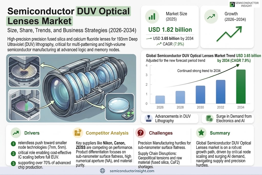
Global Semiconductor DUV Optical Lenses market size was valued at USD 1.82 billion in 2025. The market is projected to grow from USD 1.97 billion in 2026 to USD 3.65 billion by 2034, exhibiting a CAGR of 7.9% during the forecast period.
Semiconductor DUV Optical Lens is an optical component specifically used in the semiconductor manufacturing process for optical systems in the deep ultraviolet band. DUV optical lenses are commonly used in photolithography technology to transfer fine patterns using deep ultraviolet light (with wavelengths of 193nm or 248nm), which is a critical step in semiconductor microfabrication.
The market is experiencing rapid growth due to several factors, including surging investments in new semiconductor fabs, rising demand for mature-node chip production, and persistent reliance on DUV lithography for high-volume manufacturing. While EUV adoption accelerates for leading-edge nodes, DUV remains essential for cost-effective patterning at 28nm and above. Furthermore, advancements in immersion and multiple-patterning techniques bolster demand. Initiatives by key players, such as capacity expansions and material innovations, are expected to fuel further growth. Zeiss, Jenoptik, Kyocera, Newport, Seiwa Optical, Edmund Optics, Crystran, and HV Skan are some of the key players operating in the market with diverse portfolios.
MARKET DRIVERS
Advancements in Deep Ultraviolet Lithography
Semiconductor DUV optical lenses market is propelled by the relentless push toward smaller node technologies in chip manufacturing, where DUV lenses at 193nm wavelengths remain essential for high-volume production of 7nm and 5nm processes. Major foundries like TSMC and Samsung continue to rely on these precision optics for cost-effective scaling before full EUV adoption.
Surge in Demand from Electronics and AI Sectors
Growth in consumer electronics, data centers, and AI applications drives the need for high-performance semiconductors, boosting Semiconductor DUV optical lenses market. Global semiconductor sales reached approximately $520 billion in 2022, with lithography equipment demand growing at 8-10% annually, underscoring the critical role of DUV lenses in enabling complex IC designs.
➤ DUV lithography supports over 70% of advanced logic and memory chip production, ensuring supply chain stability amid EUV ramp-up delays.
Additionally, the expansion of 5G infrastructure and electric vehicles further amplifies requirements for efficient optical components, positioning the market for sustained expansion through 2030.
MARKET CHALLENGES
Precision Manufacturing Hurdles
Semiconductor DUV optical lenses market faces significant challenges in achieving sub-nanometer surface flatness and homogeneity, as even minor defects can compromise yield rates in high-end lithography scanners. Material fusion processes demand extreme purity, complicating production scalability.
Other Challenges
Supply Chain Disruptions
Geopolitical tensions and raw material shortages for fused silica and calcium fluoride have led to delivery delays, impacting 15-20% of lithography tool installations in 2023 and raising costs in the DUV optical lenses market for semiconductors.
Intensifying competition from EUV technologies also pressures DUV lens suppliers to innovate, while skilled labor shortages in optics fabrication exacerbate operational bottlenecks across the industry.
MARKET RESTRAINTS
High Development and Material Costs
Escalating expenses in R&D for next-generation semiconductor DUV optical lenses, coupled with premium pricing for low-absorption glasses, restrain market accessibility for smaller players. A single high-NA DUV lens set can exceed $100 million, limiting adoption.
Regulatory compliance for cleanroom standards and environmental controls on fluoride compounds adds further financial burdens, slowing innovation cycles in Semiconductor DUV optical lenses market.
Transition risks to EUV systems also cap long-term investments in DUV infrastructure, with projections indicating a 20-25% volume decline post-2025 for legacy nodes.
MARKET OPPORTUNITIES
Retrofit and Maintenance Services Expansion
Semiconductor DUV optical lenses market presents opportunities in aftermarket services, as existing lithography tools require periodic lens recoating and refurbishment to maintain performance, representing a $2-3 billion annual segment by 2028.
Emerging markets in Asia-Pacific, driven by new fab constructions in India and Vietnam, offer growth for localized DUV lens supply chains, potentially capturing 15% additional market share.
Hybrid DUV-EUV integration projects also create niches for advanced lenses, supporting prolonged use in multi-patterning techniques for sub-3nm nodes.
Semiconductor DUV Optical Lenses Market Trends
Advancements in Photolithography Driving Precision Enhancements
In Semiconductor DUV optical lenses market, a primary trend revolves around innovations in photolithography technology, where deep ultraviolet light at 193nm and 248nm wavelengths enables the transfer of intricate patterns onto semiconductor wafers. This process remains essential for microfabrication, with leading manufacturers like Zeiss, Jenoptik, and Newport refining lens designs to achieve superior optical performance and minimize aberrations. These developments support smaller node sizes in chip production, aligning with the demands of advanced integrated circuits.
Other Trends
Shift Toward 193nm Lens Dominance
Semiconductor DUV optical lenses market shows a clear shift toward 193nm lenses, which offer higher resolution compared to 248nm variants. This transition is propelled by the need for finer feature sizes in semiconductor manufacturing, as evidenced by segment analyses indicating stronger adoption in high-volume production environments. Key players such as Kyocera and Seiwa Optical are investing in materials like fused silica optimized for 193nm transmission, enhancing throughput and yield rates.
Expansion in Regional Markets
Geographically, Semiconductor DUV optical lenses market is witnessing robust growth in Asia, particularly in China, Japan, and South Korea, where semiconductor fabrication facilities are proliferating. North America and Europe maintain strong positions through established players like Pyramid Imaging and Crystran, focusing on customized solutions. This regional diversification mitigates supply chain risks and fosters localized innovation.
Diversification into Non-Semiconductor Applications
Beyond core semiconductor uses, Semiconductor DUV optical lenses market is diversifying into medical devices, scientific research, and other fields. Applications in precision laser systems for medical imaging and research spectroscopy leverage the lenses’ high transmission in the DUV spectrum. Manufacturers including Edmund and HV Skan are adapting products for these sectors, responding to emerging demands for compact, high-performance optics. Competitive dynamics feature top firms like Natsume and Novel holding significant shares, with ongoing mergers and developments strengthening their portfolios. Industry surveys highlight drivers such as technological miniaturization and challenges like material purity requirements, shaping strategic responses across the value chain.
COMPETITIVE LANDSCAPE
Key Industry Players
Top Manufacturers in Semiconductor DUV Optical Lenses Market
Semiconductor DUV optical lenses market is dominated by a few established players with advanced expertise in precision optics for photolithography applications, particularly at 193nm and 248nm wavelengths critical for semiconductor fabrication. Leading companies like Carl Zeiss SMT and Jenoptik hold significant market shares due to their technological leadership in high-NA DUV lens systems integrated into tools from major lithography equipment makers such as ASML and Nikon. The market structure is oligopolistic, with the global top five players accounting for a substantial portion of revenue, driven by stringent requirements for optical purity, low defect rates, and compatibility with excimer lasers. Intense R&D investments and strategic partnerships with chipmakers underscore the competitive dynamics, where innovation in CaF2 materials and coating technologies differentiates leaders.
Beyond the frontrunners, niche players contribute through specialized offerings in custom DUV lenses for semiconductor, medical, and research applications, often focusing on cost-effective solutions or regional supply chains. Companies such as Kyocera, Newport, and emerging Chinese firms like Nanjing Mloptic and Zhejiang Lante Optics are gaining traction amid supply chain diversification and rising demand from Asia-Pacific fabs. These mid-tier participants emphasize scalability, rapid prototyping, and integration with 193nm immersion systems, challenging incumbents by addressing volume needs for memory and logic chip production. The competitive landscape is evolving with mergers, capacity expansions, and a shift toward EUV transitions, yet DUV lenses remain vital for mature nodes.
List of Key Semiconductor DUV Optical Lenses Companies Profiled
- Natsume
- Zeiss
- Jenoptik
- Pyramid Imaging
- Newport
- Seiwa Optical
- Kyocera
- Edmund Optics
- Crystran
- HV Skan
- Kyocera
- Novel
- Zhejiang Lante Optics
- Nanjing Mloptic
Segment Analysis:
| Segment Category | Sub-Segments | Key Insights |
| By Type |
|
193nm Lens
|
| By Application |
|
Semiconductor
|
| By End User |
|
Foundries
|
| By Material |
|
Fused Silica
|
| By Lens Function |
|
Projection Lenses
|
Regional Analysis: Semiconductor DUV Optical Lenses Market
Asia-Pacific
Asia-Pacific’s manufacturing hubs dominate Semiconductor DUV optical lenses market through clusters in Taiwan and South Korea, where proximity to fabs enables just-in-time delivery. Specialized facilities excel in polishing and aspheric lens shaping, meeting stringent flatness tolerances required for DUV wavelengths.
Innovation thrives in the region with advancements in multi-layer anti-reflective coatings for DUV lenses, enhancing light transmission and resolution in lithography tools. Research institutions collaborate with industry to pioneer fluoride glass formulations suited for high-volume production.
A tightly knit supply chain in Asia-Pacific ensures reliability for Semiconductor DUV Optical Lenses, with vertical integration from raw materials to final assembly. This structure minimizes bottlenecks and supports scalability amid fluctuating fab utilization rates.
Substantial private and public investments fuel expansion in the region’s DUV lens sector, targeting capacity upgrades and talent development. Incentives draw global players to establish local operations, strengthening Semiconductor DUV optical lenses market ecosystem.
North America
North America plays a crucial role in Semiconductor DUV optical lenses market through its emphasis on research and development, particularly in advanced optical materials and design software. Leading firms here focus on pioneering next-generation lens architectures that improve chromatic correction for DUV applications. The region’s strengths lie in intellectual property generation and prototyping, supplying innovative solutions to global fabs. Collaborative ecosystems involving universities and equipment vendors drive refinements in lens metrology, ensuring compatibility with evolving lithography scanners. While production scales are smaller compared to Asia-Pacific, North America’s market dynamics center on high-value customization and strategic exports, supporting the broader Semiconductor DUV Optical Lenses Market with cutting-edge technologies that extend equipment lifespans.
Europe
Europe contributes significantly to Semiconductor DUV optical lenses market via specialized manufacturing expertise and precision engineering traditions. Countries like Germany and the Netherlands host facilities excelling in high-purity glass melting and coating deposition for DUV lenses. The region’s dynamics are characterized by a focus on sustainability, with efforts to develop eco-friendly production processes that reduce energy consumption in lens fabrication. Strong regulatory frameworks encourage quality assurance, positioning European suppliers as preferred partners for high-reliability applications. Partnerships with lithography toolmakers enhance integration capabilities, while R&D investments target hybrid lens designs blending DUV with emerging technologies, solidifying Europe’s niche in Semiconductor DUV optical lenses market.
South America
South America is an emerging player in Semiconductor DUV optical lenses market, with growing interest driven by increasing electronics assembly operations. Brazil and other nations are investing in basic optical component production to support local semiconductor packaging needs. Market dynamics revolve around cost-effective manufacturing and workforce training initiatives to build capabilities in lens grinding and inspection. While still nascent, regional collaborations aim to attract technology transfers, fostering gradual integration into global supply chains for DUV components. Challenges like infrastructure development are being addressed through public-private partnerships, laying groundwork for expanded participation in Semiconductor DUV optical lenses market.
Middle East & Africa
The Middle East & Africa region shows potential in Semiconductor DUV optical lenses market, particularly through diversification strategies in oil-rich economies transitioning to high-tech manufacturing. Initiatives in the UAE and Israel focus on establishing optical fabrication clusters to serve regional data center and automotive chip demands. Dynamics emphasize skill development and foreign direct investment to overcome technological gaps. Pilot projects explore DUV lens assembly tailored for harsh environments, while strategic alliances with Asian suppliers accelerate knowledge sharing. This positions the region for incremental growth in Semiconductor DUV optical lenses market amid broader economic diversification efforts.
Report Scope
This market research report provides a comprehensive analysis of Semiconductor DUV optical lenses market, covering the forecast period 2026–2034. It offers detailed insights into market dynamics, technological advancements, competitive landscape, and key trends shaping the industry.
Key focus areas of the report include:
- Market Overview: The report begins with an overview outlining its current market scenario, key growth indicators, and industry transformation drivers. It discusses macroeconomic factors, demand–supply balance, regulatory landscape, and the strategic role of semiconductors in powering advancements across industries such as automotive, telecommunications, consumer electronics, and industrial automation.
- Market Size & Forecast: Historical data and future projections for revenue, unit shipments, and market value across major regions and segments.
- Segmentation Analysis: Detailed breakdown by product type, technology, application, and end-user industry to identify high-growth segments and investment opportunities.
- Regional Insights: Insights into market performance across North America, Europe, Asia-Pacific, Latin America, and the Middle East & Africa, including country-level analysis where relevant.
- Competitive Landscape: Profiles of leading market participants, including their product offerings, R&D focus, manufacturing capacity, pricing strategies, and recent developments such as mergers, acquisitions, and partnerships.
- Technology Trends & Innovation: Assessment of emerging technologies, integration of AI/IoT, semiconductor design trends, fabrication techniques, and evolving industry standards.
- Market Drivers & Restraints: Evaluation of factors driving market growth along with challenges, supply chain constraints, regulatory issues, and market-entry barriers.
- Stakeholder Insights: Insights for component suppliers, OEMs, system integrators, investors, and policymakers regarding the evolving ecosystem and strategic opportunities.
Primary and secondary research methods are employed, including interviews with industry experts, data from verified sources, and real-time market intelligence to ensure the accuracy and reliability of the insights presented.
FREQUENTLY ASKED QUESTIONS:
What is the current market size of Semiconductor DUV Optical Lenses Market?
-> Global Semiconductor DUV Optical Lenses market was valued at USD 1.82 billion in 2025 and is projected to reach USD 3.65 billion by 2034, at a CAGR of 7.9% during the forecast period.
Which key companies operate in Semiconductor DUV Optical Lenses Market?
-> Key players include Natsume, Pyramid Imaging, Seiwa Optical, Kyocera, Edmund, Zeiss, Crystran, HV Skan, Jenoptik, Newport, among others. In 2025, the global top five players had a share approximately % in terms of revenue.
What are the key growth drivers?
-> Key growth drivers include demand in semiconductor manufacturing processes, particularly photolithography technology using deep ultraviolet light (193nm or 248nm), and expansion into medical and scientific research applications.
Which region dominates the market?
-> Asia, particularly China projected to reach USD million, is a key growth area, while North America (U.S. estimated at USD million in 2025) holds significant share.
What are the emerging trends?
-> Emerging trends include growth in the 193nm Lens segment, projected to reach USD million by 2034 at a % CAGR over the next six years, alongside diversification into semiconductor, medical, scientific research, and other applications.

Get Sample Report PDF for Exclusive Insights
Report Sample Includes
- Table of Contents
- List of Tables & Figures
- Charts, Research Methodology, and more...
 Download Sample Report PDF