
Semiconductor Digital Twin Market Insights
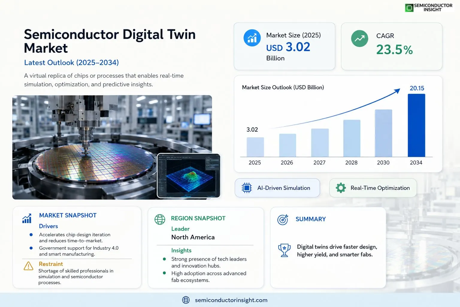
Global Semiconductor Digital Twin market size was valued at USD 3.02 billion in 2025. The market is projected to grow from USD 3.02 billion in 2025 to USD 20.15 billion by 2034, exhibiting a CAGR of 23.5% during the forecast period.A semiconductor digital twin is a highly detailed virtual replica of a physical chip or manufacturing process that mirrors real‑time performance, thermal behavior, electrical characteristics, and failure modes through advanced simulation and data analytics. By synchronizing sensor data with predictive models, engineers can explore design alternatives, optimize yield, and anticipate reliability issues before silicon fabrication.
The market is accelerating because manufacturers are embracing AI‑driven analytics, Industry 4.0 initiatives, and the need for rapid time‑to‑market cycles in advanced nodes such as sub‑10 nm technologies. Furthermore, rising demand for autonomous systems and IoT devices fuels investment in virtual prototyping platforms.
Key players,including Siemens AG, Intel Corporation, IBM Corporation, TSMC Limited, and Ansys Inc.,are expanding their portfolios through strategic partnerships and acquisitions; for example, Siemens announced a collaboration with TSMC in March 2024 to integrate digital twin capabilities into leading‑edge wafer fab workflows.
MARKET DRIVERS
Increasing Adoption of Digital Twin in Chip Design
Semiconductor Digital Twin Market is being propelled by manufacturers seeking to reduce time‑to‑market for advanced nodes. By creating virtual replicas of wafers and process equipment, firms can simulate design variations and predict yield impacts, cutting prototype cycles by up to 30%.
Regulatory Push for Smart Manufacturing
Governments worldwide are incentivizing Industry 4.0 initiatives, and digital‑twin‑enabled fabs qualify for tax credits and grants. This policy environment encourages capital investment, driving market revenue growth at an estimated CAGR of roughly 20% through 2030.
➤ “Digital twins are set to become the backbone of predictive manufacturing, unlocking efficiency gains that were previously unattainable.”
As chip complexity escalates, the need for real‑time process optimization becomes critical, positioning Semiconductor Digital Twin Market as a strategic enabler for both cost reduction and product innovation.
MARKET CHALLENGES
Complex Integration with Legacy Systems
Many fabs still rely on decades‑old equipment that lacks open APIs, making seamless data exchange with digital‑twin platforms difficult. This integration barrier can extend deployment timelines and inflate project budgets.
Other Challenges
High Development Costs
Creating accurate physics‑based models for cutting‑edge processes demands significant R&D spend and specialized talent, which can deter smaller players from entering the market.
MARKET RESTRAINTS
Limited Skilled Workforce
The scarcity of engineers proficient in both semiconductor processing and advanced simulation tools constrains rapid adoption, as firms must invest heavily in training or recruiting to fully leverage digital‑twin capabilities.
MARKET OPPORTUNITIES
Emerging Edge AI Applications
Growth in edge AI drives demand for ultra‑efficient chips, prompting designers to use digital twins for thermal and power optimization. This creates a sizable niche where Semiconductor Digital Twin Market can capture new revenue by delivering tailored simulation solutions for next‑generation AI hardware.
Semiconductor Digital Twin Market Trends
AI‑Driven Predictive Analytics Accelerate Chip Development
Semiconductor Digital Twin Market is being reshaped by AI‑enabled simulation engines that fuse real‑time sensor streams with machine‑learning models. Manufacturers now run thousands of virtual experiments on a single chip design, evaluating thermal gradients, electrical drift, and reliability margins before silicon is ever fabricated. This capability shortens design cycles, reduces costly mask iterations, and improves first‑pass yield, especially for sub‑10 nm nodes where process windows are tight. Industry 4.0 initiatives reinforce this shift, as factories adopt closed‑loop control systems that automatically adjust process parameters based on twin predictions, delivering consistent performance across high‑volume production lines.
Other Trends
Real‑Time Process Monitoring
Integrating high‑resolution sensor data with digital twin platforms provides an uninterrupted view of wafer fab health. Engineers can detect deviations in temperature, pressure, or chemical composition within seconds, triggering predictive alerts that pre‑empt defect formation. This proactive approach not only safeguards yield but also enables dynamic re‑optimization of equipment set‑points, extending tool life and lowering operational expenditures. The convergence of edge computing and twin analytics is making such monitoring scalable across globally distributed fabs, ensuring that insights derived in one location can be instantly replicated elsewhere.
Collaborative Platforms and Ecosystem Expansion
Strategic alliances among leading silicon vendors, software providers, and cloud operators are expanding the reach of Semiconductor Digital Twin Market. Joint development programs combine native design‑tool integrations with SaaS‑based analytics, allowing smaller design houses to access enterprise‑grade twin capabilities without large capital outlays. Moreover, open APIs are fostering a marketplace of third‑party modules for reliability forecasting, security assessment, and autonomous design space exploration. This ecosystem effect accelerates adoption across automotive, IoT, and edge‑compute segments, where rapid time‑to‑market and stringent reliability standards drive demand for virtual prototyping.
COMPETITIVE LANDSCAPEKey Industry Players
Semiconductor Digital Twin Market Competitive Landscape: Strategic Positioning, Key Players, and Market Dynamics Shaping the Industry Through 2034
Global Semiconductor Digital Twin market is characterized by a highly competitive and technology-intensive landscape, with a select group of dominant players commanding significant market share through robust R&D investments, strategic partnerships, and continuous portfolio expansion. Siemens AG stands out as a frontrunner in this space, leveraging its comprehensive Xcelerator digital business platform to deliver end-to-end semiconductor design and manufacturing simulation capabilities. In March 2024, Siemens reinforced its market leadership by entering a strategic collaboration with TSMC Limited to integrate advanced digital twin capabilities directly into leading-edge wafer fabrication workflows, setting a strong precedent for platform-level convergence. Ansys Inc. complements this competitive tier with its physics-based simulation tools widely adopted for chip thermal analysis, reliability modeling, and process optimization across sub-10 nm technology nodes. Intel Corporation and IBM Corporation further solidify the upper competitive tier by embedding digital twin methodologies into their respective chip design and AI-driven analytics ecosystems, supporting rapid time-to-market cycles critical in next-generation semiconductor development.Beyond the leading incumbents, a diverse set of niche and emerging players are actively shaping Semiconductor Digital Twin Market by addressing specialized segments such as virtual prototyping, yield enhancement, and IoT-driven process control. Synopsys and Cadence Design Systems bring deep electronic design automation expertise that increasingly converges with digital twin frameworks for pre-silicon verification and process simulation. NVIDIA Corporation is gaining traction through its Omniverse platform, which enables photorealistic, real-time digital twin environments applicable to semiconductor fab modeling. ASML Holding, as the world’s leading supplier of lithography equipment, is progressively integrating digital twin solutions to optimize scanner performance and predictive maintenance within advanced fabs. Companies such as Dassault Systèmes, PTC Inc., and Rockwell Automation contribute industrial digital twin platforms adaptable to semiconductor manufacturing environments, while specialized simulation firms including Coventor (a Lam Research company) and PDF Solutions focus specifically on process-level twin modeling and wafer yield analytics. Collectively, these players are accelerating market growth, which is projected to rise from USD 3.02 billion in 2025 to USD 20.15 billion by 2034, at a CAGR of 23.5%.
List of Key Semiconductor Digital Twin Companies Profiled
- Siemens AG
- Intel Corporation
- IBM Corporation
- Ansys Inc.
- TSMC Limited
- Synopsys Inc.
- Cadence Design Systems
- NVIDIA Corporation
- ASML Holding N.V.
- Dassault Systèmes SE
- PTC Inc.
- Rockwell Automation Inc.
- Coventor Inc. (a Lam Research Company)
- PDF Solutions Inc.
- Onto Innovation Inc.
Segment Analysis:
| Segment Category | Sub-Segments | Key Insights |
| By Type |
|
Physical Chip Twin dominates because it provides a concrete, geometry‑level replica that engineers can interrogate throughout the design lifecycle.
|
| By Application |
|
Yield Optimization is the primary driver for adopting digital twins in semiconductor fabs.
|
| By End User |
|
Semiconductor Manufacturers lead the market because they own the end‑to‑end production ecosystem.
|
| By Technology |
|
AI‑Driven Modeling emerges as the leading technology due to its ability to learn from vast sensor streams and predict complex interactions.
|
| By Value Chain Stage |
|
Fabrication stands out as the segment where digital twins deliver the most tangible operational advantage.
|
Regional Analysis: North America
North America
North America has a strong emphasis on utilizing semiconductor digital twins for early-stage design and simulation. This enables engineers to virtually prototype and test designs, leading to faster iterations and reduced physical prototyping costs.
Semiconductor manufacturers in North America are leveraging digital twins to optimize their manufacturing processes. This includes simulating production lines, identifying bottlenecks, and improving overall yield and efficiency. Predictive analytics within these twins help in proactive maintenance, minimizing downtime.
The advanced semiconductor industry in North America heavily relies on digital twins for predictive maintenance of complex equipment. By monitoring real-time data and simulating potential failures, companies can proactively schedule maintenance, reducing unexpected disruptions and extending equipment lifespan.
North American semiconductor companies are increasingly using digital twins to model and optimize their complex supply chains. This allows for better forecasting, risk mitigation, and improved responsiveness to market changes.
North America
The North American semiconductor digital twin market is experiencing significant investment in advanced technologies to bolster its competitive edge. The strong presence of companies like Intel, Nvidia, and AMD drives innovation and adoption. A key trend is the growing integration of digital twins with metaverse technologies, creating immersive environments for design review and collaboration. This region is also a hub for research and development, with numerous universities and research institutions contributing to the advancement of digital twin capabilities for semiconductor applications. The focus extends beyond individual device design to encompass entire manufacturing ecosystems, reflecting a strategic shift toward holistic operational improvements. This necessitates robust data analytics and cybersecurity measures within the digital twin framework.
Europe
Europe’s semiconductor industry, while facing certain economic headwinds, is actively embracing digital twin technology to enhance its competitiveness. The region is focusing on improving energy efficiency in semiconductor manufacturing through digital twins, aligning with sustainability goals. Collaboration between industry players and research institutions is fostering innovation in areas such as process optimization and yield prediction. The European Union’s initiatives to support advanced manufacturing are further driving the adoption of these technologies. Emphasis is placed on developing digital twin solutions that comply with stringent data privacy regulations.
Asia-Pacific
Asia-Pacific, particularly China, is emerging as a dominant force in Semiconductor Digital Twin Market. The rapid expansion of the semiconductor industry in this region, coupled with government support for advanced manufacturing, is fueling strong demand. Digital twins are being utilized to optimize large-scale manufacturing facilities and accelerate the development of next-generation semiconductor devices. Investment in AI and machine learning capabilities within digital twins is a key focus. The market is characterized by a high volume of adoption across various semiconductor applications, from memory chips to advanced logic circuits.
South America
The semiconductor industry in South America is relatively nascent but shows promising growth potential. Limited investment in digital twin technologies currently exists, but there is increasing awareness of the benefits for optimizing existing manufacturing processes and attracting foreign investment in the sector. Initial applications are focused on basic process simulation and equipment monitoring. Government initiatives to promote technological advancement are expected to drive greater adoption in the coming years.
Middle East & Africa
The semiconductor market in the Middle East and Africa is still in its early stages. While there are limited existing digital twin deployments, there is growing interest in leveraging these technologies to support the development of local semiconductor manufacturing capabilities. Focus areas include optimizing supply chains and improving operational efficiency in existing electronics manufacturing facilities. Government investments in technology and infrastructure are expected to create opportunities for digital twin solutions in the region.
Report Scope
This market research report provides a comprehensive analysis of the Semiconductor Digital Twin Market , covering the forecast period 2026–2034. It offers detailed insights into market dynamics, technological advancements, competitive landscape, and key trends shaping the industry.
Key focus areas of the report include:
- Market Overview: The report begins with an overview outlining its current market scenario, key growth indicators, and industry transformation drivers. It discusses macroeconomic factors, demand–supply balance, regulatory landscape, and the strategic role of semiconductors in powering advancements across industries such as automotive, telecommunications, consumer electronics, and industrial automation.
- Market Size & Forecast: Historical data and future projections for revenue, unit shipments, and market value across major regions and segments.
- Segmentation Analysis: Detailed breakdown by product type, technology, application, and end-user industry to identify high-growth segments and investment opportunities.
- Regional Insights: Insights into market performance across North America, Europe, Asia-Pacific, Latin America, and the Middle East & Africa, including country-level analysis where relevant.
- Competitive Landscape: Profiles of leading market participants, including their product offerings, R&D focus, manufacturing capacity, pricing strategies, and recent developments such as mergers, acquisitions, and partnerships.
- Technology Trends & Innovation: Assessment of emerging technologies, integration of AI/IoT, semiconductor design trends, fabrication techniques, and evolving industry standards.
- Market Drivers & Restraints: Evaluation of factors driving market growth along with challenges, supply chain constraints, regulatory issues, and market-entry barriers.
- Stakeholder Insights: Insights for component suppliers, OEMs, system integrators, investors, and policymakers regarding the evolving ecosystem and strategic opportunities.
Primary and secondary research methods are employed, including interviews with industry experts, data from verified sources, and real-time market intelligence to ensure the accuracy and reliability of the insights presented.
FREQUENTLY ASKED QUESTIONS:
What is the current market size of Semiconductor Digital Twin Market?
-> Semiconductor Digital Twin Market was valued at USD 3.02 billion in 2025 and is expected to reach USD 20.15 billion by 2034.
Which key companies operate in Semiconductor Digital Twin Market?
-> Key players include Axalta Coating Systems, AkzoNobel, BASF SE, PPG, Sherwin-Williams, and 3M, among others.
What are the key growth drivers?
-> Key growth drivers include railway infrastructure investments, urbanization, and demand for durable coatings.
Which region dominates the market?
-> Asia-Pacific is the fastest-growing region, while Europe remains a dominant market.
What are the emerging trends?
-> Emerging trends include bio-based coatings, smart coatings, and sustainable rail solutions.

Get Sample Report PDF for Exclusive Insights
Report Sample Includes
- Table of Contents
- List of Tables & Figures
- Charts, Research Methodology, and more...
 Download Sample Report PDF





