MARKET INSIGHTS
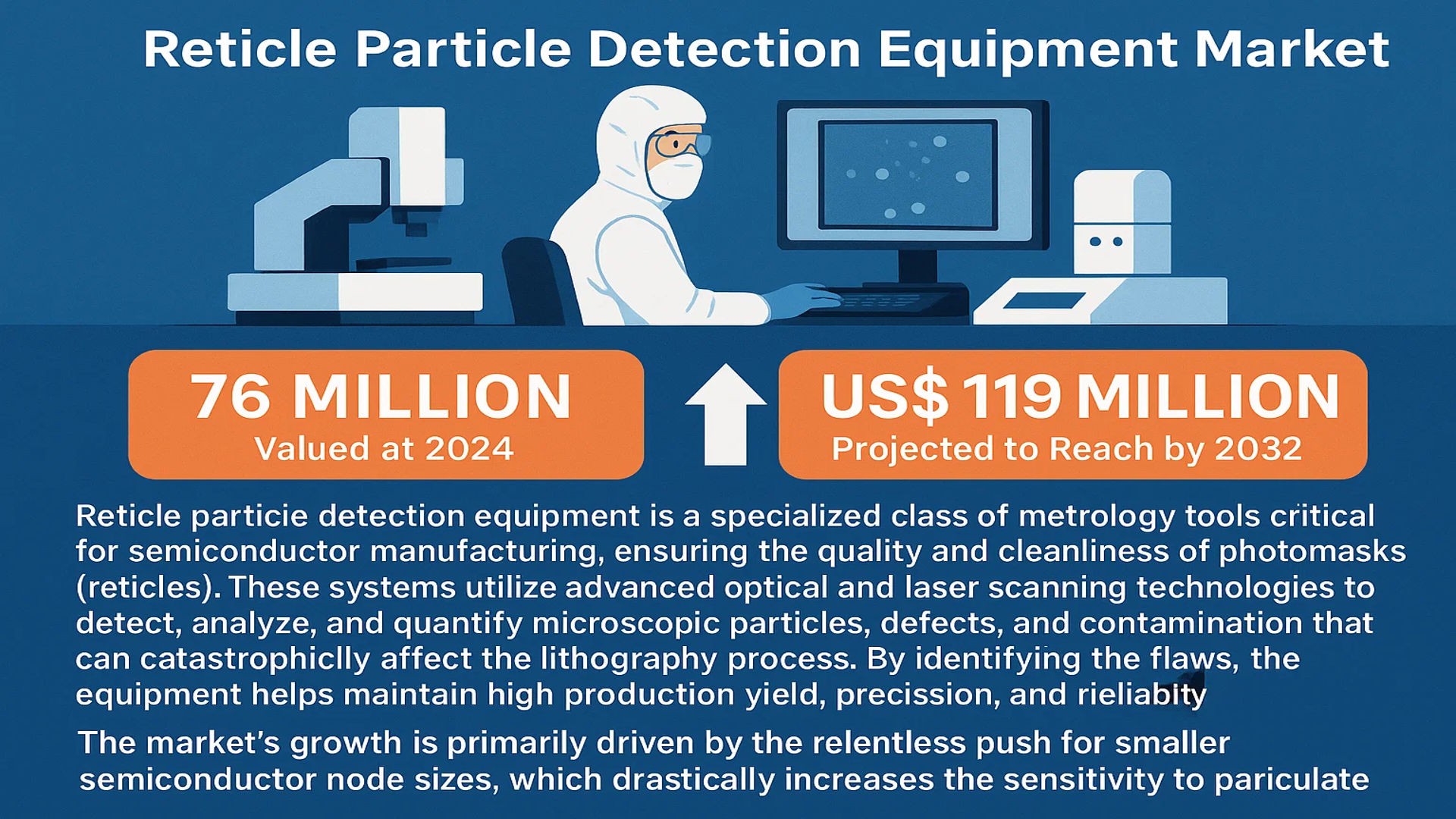
The global Reticle Particle Detection Equipment Market was valued at 76 million in 2024 and is projected to reach US$ 119 million by 2032, at a CAGR of 6.8% during the forecast period.
Reticle particle detection equipment is a specialized class of metrology tools critical for semiconductor manufacturing, ensuring the quality and cleanliness of photomasks (reticles). These systems utilize advanced optical and laser scanning technologies to detect, analyze, and quantify microscopic particles, defects, and contamination that can catastrophically affect the lithography process. By identifying these flaws, the equipment helps maintain high production yield, precision, and reliability in advanced device fabrication.
The market’s growth is primarily driven by the relentless push for smaller semiconductor node sizes, which drastically increases the sensitivity to particulate contamination. Furthermore, the expansion of high-volume manufacturing facilities, particularly for memory and logic chips, and stringent quality control mandates from foundries are significant contributors. The competitive landscape is dominated by key players such as KLA Corporation and Lasertec Corporation, who continuously innovate to offer systems with higher resolution and throughput to meet the industry’s evolving demands.
MARKET DYNAMICS
MARKET DRIVERS
Increasing Semiconductor Miniaturization and Complexity to Drive Market Growth
The relentless push toward semiconductor miniaturization, with nodes now reaching 3nm and below, is significantly driving demand for reticle particle detection equipment. As feature sizes shrink to atomic scales, even nanometer-sized particles can cause catastrophic defects during lithography, making contamination control absolutely critical. The transition to extreme ultraviolet (EUV) lithography has further amplified this need, as EUV reticles are particularly sensitive to contamination due to their reflective multilayer structure. Semiconductor manufacturers are investing heavily in advanced detection systems to maintain yield rates, with some estimates suggesting that a single particle-related defect can cost up to $50,000 in lost production. This technological imperative, combined with the global semiconductor market’s projected growth to over $1 trillion by 2030, creates sustained demand for sophisticated particle detection solutions.
Rising Quality Standards and Yield Optimization Requirements to Boost Adoption
The semiconductor industry’s increasing focus on yield optimization and quality assurance is driving substantial investments in reticle particle detection equipment. With manufacturing costs for advanced nodes exceeding $20 billion per fab, even marginal yield improvements justify significant capital expenditure on contamination control. Modern detection systems can identify particles as small as 50 nanometers, providing the sensitivity required for today’s most advanced processes. The implementation of Industry 4.0 and smart manufacturing principles has further enhanced the value proposition of these systems, enabling real-time monitoring and predictive maintenance. As foundries compete to achieve yield rates above 90% for complex chips, the demand for advanced particle detection technology continues to grow, particularly in memory and logic semiconductor segments where defect tolerance is extremely low.
Expansion of Semiconductor Manufacturing Capacity to Fuel Market Expansion
Global semiconductor capacity expansion, particularly in Asia and North America, is creating substantial opportunities for reticle particle detection equipment suppliers. The CHIPS Act in the United States has committed over $50 billion toward domestic semiconductor manufacturing, while similar initiatives in the European Union and various Asian countries are driving fab construction worldwide. Each new fabrication facility represents potential demand for multiple particle detection systems, with larger fabs requiring dozens of units across different process stages. The ongoing geopolitical emphasis on semiconductor sovereignty ensures that this capacity expansion trend will continue through the decade, providing a stable long-term growth driver for detection equipment manufacturers. This capacity build-out coincides with technological transitions to more advanced nodes, further increasing the per-fab requirement for sophisticated contamination control systems.
MARKET CHALLENGES
High Capital Investment and Operational Costs to Challenge Market Penetration
The significant capital investment required for advanced reticle particle detection systems presents a substantial challenge for market growth, particularly for smaller semiconductor manufacturers and research facilities. State-of-the-art detection equipment can cost several million dollars per unit, placing them beyond the reach of many potential customers. Beyond the initial purchase price, these systems require specialized facilities, regular maintenance, and highly trained operators, adding considerable operational expenses. The total cost of ownership for a comprehensive particle detection setup can exceed $10 million over five years, making justification difficult for facilities with limited production volumes or less critical contamination requirements. This financial barrier particularly affects emerging semiconductor regions and academic institutions, limiting market expansion potential.
Other Challenges
Technical Complexity and Integration Difficulties
Integrating particle detection systems into existing semiconductor manufacturing workflows presents significant technical challenges. These systems must interface with various other equipment types, including lithography tools, metrology systems, and factory automation software. Compatibility issues can arise between equipment from different vendors, requiring custom integration solutions that increase implementation time and cost. The need for minimal disruption to production operations during installation and calibration further complicates deployment, often requiring planned downtime that can cost facilities thousands of dollars per hour.
Rapid Technological Obsolescence
The pace of semiconductor technology advancement creates constant pressure for detection equipment upgrades. Systems purchased today may become inadequate within three to five years as process nodes advance and contamination requirements tighten. This rapid obsolescence cycle makes capital investment decisions challenging for manufacturers, who must balance current needs against future requirements. The need for frequent technology refresh cycles increases the total cost of ownership and can delay purchase decisions, particularly during periods of economic uncertainty or industry consolidation.
MARKET RESTRAINTS
Limited Technical Expertise and Specialized Workforce Shortages to Deter Market Growth
The semiconductor industry’s rapid growth has created a significant shortage of technical professionals with expertise in particle detection and contamination control. Operating advanced detection equipment requires specialized knowledge in optics, particle physics, semiconductor processes, and data analysis. The global semiconductor workforce shortage, estimated at over one million skilled workers by 2030, particularly affects highly specialized roles such as particle detection system operators and maintenance engineers. This skills gap is exacerbated by the retirement of experienced technicians and the time required to train new personnel, which can take six to twelve months for basic competency and several years for full proficiency. The shortage of qualified professionals limits the effective deployment and utilization of detection systems, restraining market growth despite strong underlying demand.
Cyclical Nature of Semiconductor Industry to Create Demand Volatility
The semiconductor industry’s well-known cyclicality presents a significant restraint for reticle particle detection equipment manufacturers. During industry downturns, capital expenditure is typically among the first budget items reduced or delayed, directly affecting equipment purchases. The memory segment, in particular, experiences severe cycles of overcapacity and undersupply, causing dramatic fluctuations in equipment demand. Historical patterns show that semiconductor capital spending can decline by 20-30% during downturn periods, with equipment manufacturers experiencing even steeper revenue reductions. This volatility makes long-term planning and capacity investment challenging for detection equipment suppliers, who must maintain technical expertise and manufacturing capability through periods of reduced demand. The industry’s cyclical nature also affects customer payment terms and equipment financing availability, further complicating market stability.
Stringent Certification and Qualification Processes to Slow Market Adoption
The extensive qualification and certification requirements for new detection equipment significantly restrain market growth by extending sales cycles and increasing development costs. Semiconductor manufacturers typically require six to twelve months of rigorous testing before approving new equipment for production use, involving multiple validation stages and extensive documentation. This process ensures that detection systems meet strict performance, reliability, and compatibility standards but creates substantial barriers for new market entrants and technology upgrades. The qualification requirements are particularly stringent for leading-edge nodes, where equipment performance directly affects multi-billion-dollar production investments. These extended adoption timelines delay revenue recognition for equipment suppliers and can cause technology to become outdated during the qualification process, particularly in rapidly advancing semiconductor segments.
MARKET OPPORTUNITIES
Integration of Artificial Intelligence and Machine Learning to Create New Value Propositions
The integration of artificial intelligence and machine learning technologies presents significant opportunities for enhancing reticle particle detection capabilities and creating new market segments. AI-powered systems can improve detection accuracy by distinguishing between critical particles and false positives, reducing unnecessary reticle cleaning and inspection cycles. Machine learning algorithms can predict contamination trends and recommend preventive measures, moving from detection to prevention strategies. These advanced capabilities enable semiconductor manufacturers to achieve higher yields and reduce operational costs, creating willingness to pay premium prices for intelligent detection solutions. The adoption of AI-enhanced systems is particularly valuable for high-volume manufacturing facilities where even minor yield improvements can generate additional revenue exceeding the equipment cost within months.
Expansion into Emerging Semiconductor Regions to Drive Geographic Growth
The strategic expansion of semiconductor manufacturing into new geographic regions creates substantial opportunities for reticle particle detection equipment suppliers. Countries across Southeast Asia, the Middle East, and Latin America are developing domestic semiconductor capabilities as part of economic diversification and technology sovereignty initiatives. These emerging semiconductor regions typically begin with mature technology nodes where contamination control requirements are less stringent but gradually advance to more sophisticated processes requiring advanced detection systems. The establishment of new semiconductor clusters creates greenfield opportunities for equipment suppliers to establish long-term customer relationships and capture market share before competitors establish strong presence. This geographic expansion is supported by government incentives and international partnerships, ensuring sustained investment in semiconductor infrastructure over the coming decade.
Development of Multi-Function Inspection Platforms to Address Comprehensive Quality Needs
The convergence of particle detection with other inspection and metrology functions creates opportunities for integrated solutions that address broader quality control requirements. Modern semiconductor manufacturers seek to reduce equipment footprint and simplify operations by combining multiple inspection functions into single platforms. Advanced systems that integrate particle detection, pattern defect identification, dimensional metrology, and surface characterization offer significant value by providing comprehensive quality assessment while reducing capital investment and operational complexity. The development of these multi-function platforms requires deep technical expertise across multiple inspection domains but creates strong customer loyalty and recurring revenue opportunities through service contracts and consumables. This trend toward integrated solutions is particularly relevant for advanced packaging and heterogeneous integration applications, where traditional inspection approaches face limitations.
RETICLE PARTICLE DETECTION EQUIPMENT MARKET TRENDS
Increasing Miniaturization and Complexity of Semiconductor Nodes Drives Market Adoption
The relentless push towards smaller semiconductor nodes, now moving into the 3nm and 2nm realms, has fundamentally elevated the importance of reticle cleanliness. At these advanced nodes, even a single sub-micron particle can cause catastrophic defects, rendering an entire wafer useless and impacting fab yield rates that are already under immense pressure. This has created a non-negotiable demand for highly sophisticated particle detection equipment capable of identifying contaminants as small as 50 nanometers with extreme precision. The market is responding with systems that integrate advanced laser scattering techniques, enhanced imaging sensors, and automated handling to minimize human-induced contamination. This trend is directly linked to the multi-billion-dollar investments in new fabrication facilities globally, where equipping a production line with state-of-the-art inspection tools is a standard prerequisite for high-volume manufacturing.
Other Trends
Integration of Artificial Intelligence and Machine Learning
The integration of Artificial Intelligence (AI) and Machine Learning (ML) is revolutionizing defect classification and analysis, moving beyond simple detection to predictive maintenance and root cause analysis. Modern systems are now trained on vast datasets of defect images, enabling them to not only identify a particle but also categorize its type—be it organic residue, a silicon fragment, or a metal flake—with over 99% accuracy. This intelligent analysis drastically reduces false positives and accelerates the decision-making process for cleaning or rejecting a reticle. Furthermore, ML algorithms are being deployed to predict equipment maintenance needs by analyzing performance drift over time, thereby minimizing unplanned downtime and ensuring consistent throughput. This shift towards smart, data-driven inspection is becoming a critical differentiator for equipment manufacturers.
Rising Demand for Integrated Particle Removal Systems
There is a growing market preference for systems that combine detection with in-situ particle removal capabilities, a segment projected for significant growth. The traditional workflow of detecting contamination on a separate tool and then transferring the reticle to a cleaning station increases handling time and the risk of further damage or contamination. Integrated solutions streamline this process, offering a closed-loop system where detection immediately triggers a non-contact cleaning process, often using precise laser or cryogenic aerosol techniques. This trend is particularly strong in high-volume mask shops and semiconductor manufacturing sites where throughput and reticle availability are paramount. The efficiency gains from reducing handling steps and minimizing cross-contamination risks are substantial, making these integrated systems a highly attractive investment for manufacturers aiming to optimize their lithography cell operations and protect their multi-million-dollar reticle inventories.
COMPETITIVE LANDSCAPE
Key Industry Players
Technological Innovation and Strategic Expansion Drive Market Leadership
The global reticle particle detection equipment market exhibits a semi-consolidated competitive structure, characterized by the presence of established multinational corporations, specialized technology firms, and emerging regional players. KLA Corporation stands as the undisputed market leader, commanding a significant revenue share due to its comprehensive portfolio of advanced inspection systems, including the Teron 600 series, and its entrenched relationships with major semiconductor foundries. The company’s dominance is further solidified by its extensive service network and continuous R&D investments, which exceeded $1.2 billion in 2023, focusing on enhancing detection sensitivity for next-generation nodes.
Lasertec Corporation and Carl Zeiss AG also hold considerable market influence, particularly in the extreme ultraviolet (EUV) lithography segment. Lasertec’s strength lies in its proprietary actinic pattern inspection technology, which is critical for EUV mask quality control, while Zeiss leverages its expertise in optics and metrology to provide high-resolution imaging solutions. Both companies have reported increased capital expenditures to expand production capacity in response to growing demand from advanced logic and memory manufacturers.
Meanwhile, Applied Materials, Inc. and HORIBA, Ltd. are strengthening their positions through strategic initiatives and product diversification. Applied Materials integrates particle detection within its larger semiconductor manufacturing ecosystem, offering bundled solutions that improve operational efficiency for customers. HORIBA focuses on analytical instrumentation, with recent developments in laser-induced breakdown spectroscopy (LIBS) for contamination analysis. These players are actively pursuing partnerships with research institutions and industry consortia to co-develop standards and technologies addressing sub-10nm particle detection challenges.
The competitive landscape is further energized by agile specialized firms and regional champions. Companies like Advanced Technology Inc. (South Korea) and Shanghai Yuwei Semiconductor Technology (China) are growing rapidly by offering cost-effective solutions tailored to local market needs, supported by government initiatives to strengthen domestic semiconductor supply chains. Their expansion strategies include targeting mid-tier semiconductor manufacturers and mask shops seeking reliable alternatives to premium-priced equipment.
List of Key Reticle Particle Detection Equipment Companies Profiled
- KLA Corporation (U.S.)
- HORIBA, Ltd. (Japan)
- Lasertec Corporation (Japan)
- Advanced Technology Inc. (South Korea)
- Applied Materials, Inc. (U.S.)
- Fastmicro (Germany)
- Carl Zeiss AG (Germany)
- LAZIN (U.S.)
- VPTek (South Korea)
- Shanghai Yuwei Semiconductor Technology Co., Ltd. (China)
- Zhuhai Chengfeng Electronic Technology Co., Ltd. (China)
Segment Analysis:
By Type
Systems with Particle Removal Dominate Due to Integrated Cleaning Capabilities Enhancing Production Yield
The market is segmented based on type into:
- With Particle Removal
- Without Particle Removal
By Application
Semiconductor Chip Manufacturer Segment Leads Due to Critical Need for Defect-Free Reticles in Advanced Node Production
The market is segmented based on application into:
- Semiconductor Chip Manufacturer
- Mask Factory
- Others
By Technology
Laser-Based Inspection Systems Hold Significant Share Owing to High Sensitivity and Speed
The market is segmented based on technology into:
- Laser Scattering Technology
- Image Processing Technology
- Others
By Automation Level
Fully Automated Systems are Gaining Traction for High-Volume Manufacturing Facilities
The market is segmented based on automation level into:
- Fully Automated Systems
- Semi-Automated Systems
- Manual Systems
Regional Analysis: Reticle Particle Detection Equipment Market
Asia-Pacific
The Asia-Pacific region is the undisputed leader in the global Reticle Particle Detection Equipment market, driven by its dominant semiconductor manufacturing ecosystem. Countries like Taiwan, South Korea, and China are global powerhouses in chip fabrication, hosting the world’s leading foundries such as TSMC and Samsung Electronics. This concentration of high-volume, advanced-node production creates an immense and non-negotiable demand for the highest quality reticle inspection to protect multi-billion-dollar fabrication lines from yield loss. While China is aggressively expanding its domestic semiconductor capacity as part of its national strategy, countries like Japan remain critical due to their strong presence in the photomask and equipment supply chain, with companies like Lasertec Corporation being key innovators. The region’s growth is further fueled by massive government investments and initiatives aimed at achieving semiconductor self-sufficiency, making it the primary driver of both volume and technological advancement in this market.
North America
North America, particularly the United States, represents a high-value market characterized by technological innovation and strategic reshoring initiatives. The region is home to major global equipment manufacturers like KLA and Applied Materials, whose R&D efforts set the global standard for detection sensitivity and speed. The recent CHIPS and Science Act, which allocates over $52 billion in funding for domestic semiconductor research and manufacturing, is a significant catalyst. This legislation is directly spurring investments in new fab constructions and expansions by companies like Intel and GlobalFoundries, which in turn will require advanced reticle inspection tools to ensure production integrity. The market demand here is heavily skewed towards the most sophisticated equipment capable of handling the extreme ultraviolet (EUV) lithography processes that are becoming standard for leading-edge nodes, emphasizing performance over cost.
Europe
The European market is steadily growing, supported by the EU’s concerted efforts to bolster its semiconductor sovereignty through the European Chips Act. While the region’s manufacturing footprint is smaller than Asia’s, it includes strategically important facilities from companies like STMicroelectronics and Infineon, which specialize in advanced analog, power, and automotive chips. These applications require highly reliable reticles, sustaining consistent demand for detection equipment. Furthermore, Europe hosts several prominent research institutes and equipment suppliers, such as Zeiss, which play a crucial role in developing next-generation inspection technologies. The market’s evolution is closely tied to the success of large-scale pan-European projects aimed at reducing dependency on external supply chains, making it a region focused on building long-term, sustainable capability.
South America
The market for Reticle Particle Detection Equipment in South America is nascent and limited. The region lacks a significant semiconductor fabrication presence, with most chip consumption being met through imports. Local industrial activity is more focused on assembly, testing, and packaging rather than the front-end manufacturing that requires photomasks. Consequently, demand for this highly specialized equipment is minimal and is primarily driven by a handful of research laboratories, academic institutions, and perhaps small-scale operations serving specific industrial electronics needs. Market growth is constrained by economic factors and the absence of a coordinated national or regional strategy to develop a local semiconductor fabrication industry, making it a minor player in the global landscape.
Middle East & Africa
Similar to South America, the Middle East and Africa region has a very underdeveloped market for this equipment. While some nations, particularly in the Gulf Cooperation Council (GCC), have immense financial resources and ambitions to diversify their economies beyond oil, investments have historically targeted larger-scale infrastructure and technology adoption rather than foundational semiconductor manufacturing. Any existing demand would be isolated to highly specialized technology hubs or universities engaged in microelectronics research. However, the extreme cost and expertise required to operate and maintain reticle inspection equipment pose significant barriers. Therefore, this region currently represents a potential long-term opportunity rather than a current source of significant market demand.
Report Scope
This market research report provides a comprehensive analysis of the global and regional Reticle Particle Detection Equipment markets, covering the forecast period 2025–2032. It offers detailed insights into market dynamics, technological advancements, competitive landscape, and key trends shaping the industry.
Key focus areas of the report include:
- Market Size & Forecast: Historical data and future projections for revenue, unit shipments, and market value across major regions and segments.
- Segmentation Analysis: Detailed breakdown by product type, technology, application, and end-user industry to identify high-growth segments and investment opportunities.
- Regional Outlook: Insights into market performance across North America, Europe, Asia-Pacific, Latin America, and the Middle East & Africa, including country-level analysis where relevant.
- Competitive Landscape: Profiles of leading market participants, including their product offerings, R&D focus, manufacturing capacity, pricing strategies, and recent developments such as mergers, acquisitions, and partnerships.
- Technology Trends & Innovation: Assessment of emerging technologies, integration of AI/IoT, semiconductor design trends, fabrication techniques, and evolving industry standards.
- Market Drivers & Restraints: Evaluation of factors driving market growth along with challenges, supply chain constraints, regulatory issues, and market-entry barriers.
- Stakeholder Analysis: Insights for component suppliers, OEMs, system integrators, investors, and policymakers regarding the evolving ecosystem and strategic opportunities.
Primary and secondary research methods are employed, including interviews with industry experts, data from verified sources, and real-time market intelligence to ensure the accuracy and reliability of the insights presented.
FREQUENTLY ASKED QUESTIONS:
What is the current market size of Global Reticle Particle Detection Equipment Market?
-> Reticle Particle Detection Equipment Market was valued at 76 million in 2024 and is projected to reach US$ 119 million by 2032, at a CAGR of 6.8% during the forecast period.
Which key companies operate in Global Reticle Particle Detection Equipment Market?
-> Key players include KLA, HORIBA, Lasertec Corporation, Applied Materials, and Zeiss, among others.
What are the key growth drivers?
-> Key growth drivers include increasing semiconductor manufacturing complexity, demand for higher chip yields, and stringent quality control requirements in advanced lithography processes.
Which region dominates the market?
-> Asia-Pacific is the dominant market, driven by major semiconductor manufacturing hubs in Taiwan, South Korea, and China.
What are the emerging trends?
-> Emerging trends include integration of AI for defect classification, automation for inline metrology, and development of systems for EUV lithography mask inspection.

Get Sample Report PDF for Exclusive Insights
Report Sample Includes
- Table of Contents
- List of Tables & Figures
- Charts, Research Methodology, and more...