Resist Processing Equipment Market Insights
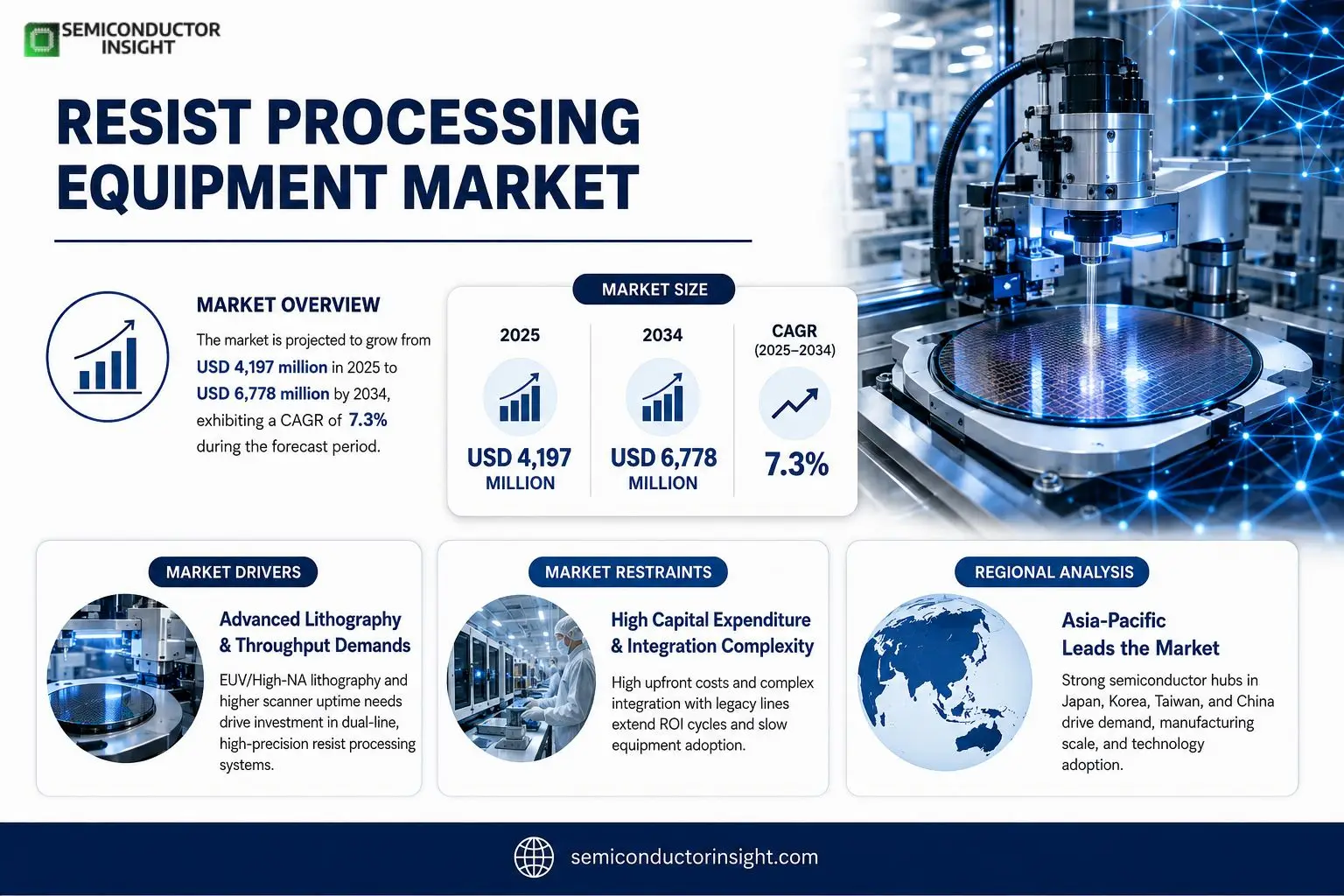
Resist Processing Equipment market size was valued at USD 4,197 million in 2025. The market is projected to grow from USD 4,197 million in 2025 to USD 6,778 million by 2034, exhibiting a CAGR of 7.3% during the forecast period.
Resist Processing Systems refer to integrated coat‑/develop “track” tools that sit beside stepper or scanner units inside a lithography cell. A typical track combines spin or spray coating, edge‑bead removal, soft‑bake/PEB/chill conditioning, puddle or spray develop, rinse/dry modules and robotic wafer handling with FOUP/load‑port interfaces designed to match scanner takt time.The market expands because tighter defect budgets for EUV/High‑NA nodes demand higher thermal stability and throughput; manufacturers therefore favor dual‑line architectures that boost OEE while reducing downtime. Suppliers such as TEL’s CLEAN TRACK™ LITHIUS series and SCREEN’s DT‑3000 (SOKUDO DUO) are adding advanced‑node readiness and broader material compatibility to capture logic, memory and emerging packaging segments.
MARKET DRIVERS
Technological Advancements in Lithography
The adoption of extreme‑ultraviolet (EUV) lithography has forced semiconductor fabs to revisit their resist processing lines. Higher resolution demands translate into tighter tolerances for coating uniformity, prompting manufacturers to invest in next‑generation spin coaters and bake ovens. This capital shift is observable across leading fabs that have upgraded equipment within the past 12‑18 months, reflecting a clear correlation between patterning complexity and equipment refresh cycles.
Cost‑Efficiency Pressures
As wafer sizes expand to 300 mm and beyond, process throughput becomes a decisive cost lever. Modern resist processing platforms now integrate inline inspection and real‑time metrology, allowing operators to reduce scrap rates by up to 15 %. The promise of lower per‑wafer cost is a strong incentive for fabs to replace legacy tools that cannot sustain the required cycle times.
➤ “Equipment that merges coating, soft‑bake, and develop functions into a single footprint is reshaping fab floor planning and capital allocation.”
Regulatory trends toward greener manufacturing have also nudged the market. Solvent‑reduced chemistries and energy‑efficient bake chambers are being favored, driving equipment vendors to certify their offerings against emerging environmental standards. Compliance readiness therefore acts as both a market catalyst and a differentiator for suppliers.
MARKET CHALLENGES
Integration Complexity with Existing Lines
Retrofitting advanced resist processing units into legacy fabs often entails substantial re‑engineering of air handling, utilities, and workflow automation. The downtime required for validation can erode the anticipated ROI, especially for plants operating at high capacity utilization. Consequently, many manufacturers adopt a phased approach, which slows overall market momentum.
Other Challenges
Talent Shortage
Skilled technicians capable of troubleshooting high‑precision coating and bake equipment are in short supply. Training programs have not kept pace with the rapid technology turnover, leaving a gap that hampers optimal equipment utilization and extends commissioning timelines.Supply‑chain volatility, particularly for specialty gases and high‑purity chemicals, adds another layer of uncertainty. Fluctuating procurement costs can compel fabs to defer equipment upgrades, opting instead for incremental process tweaks.
MARKET RESTRAINTS
High Capital Expenditure Thresholds
The upfront outlay for state‑of‑the‑art resist processing suites often exceeds $10 million per line, a figure that can strain the CapEx budgets of mid‑size fabs. Even when financing options are available, the payback period can extend beyond the typical product lifecycle, discouraging aggressive investment.Economic headwinds in key end‑use industries, such as consumer electronics, further temper spending. A slowdown in device shipments translates to reduced wafer demand, prompting fabs to adopt a more conservative equipment refresh cadence.Regulatory compliance costs associated with waste management and emissions reporting can also inflate total ownership expense. Companies must allocate additional resources to maintain documentation and meet ever‑tightening standards, which can deter the adoption of newer, potentially greener technologies.
MARKET OPPORTUNITIES
Modular, Scalable Equipment Architectures
Vendors that deliver modular resist processing platforms enable fabs to scale capacity in line with demand, reducing the risk of over‑investment. Flexibility in configurationsuch as interchangeable coating heads or add‑on bake modulesappeals to manufacturers seeking to future‑proof their lines without committing to a monolithic purchase.Emerging applications in advanced packaging and three‑dimensional integrated circuits are creating niche demand for ultra‑thin resist layers and precise edge bead removal. Equipment optimized for these processes can capture a premium market segment, especially as OEMs push envelope‑level performance.Strategic partnerships between equipment manufacturers and resist chemistry suppliers are fostering co‑development initiatives. Joint solutions that synchronize tool parameters with material properties promise to unlock yield improvements, offering a compelling value proposition for both technology providers and end‑users.
Resist Processing Equipment Market Trends
Integrating High‑Throughput Tracks with EUV Lithography
The 300 mm multi‑module track remains the backbone of high‑volume manufacturing, yet its architecture is being reengineered to satisfy the tighter defect and thermal stability budgets that EUV and High‑NA scanners impose. Suppliers such as Tokyo Electron and SCREEN have rolled out dual‑line platformsLITHIUS Pro DICE and DT‑3000 respectivelythat double wafer‑per‑hour throughput while embedding closed‑loop temperature control and real‑time metrology to suppress pattern drift. For fabs, this translates into a direct uplift in scanner uptime because the lithography step no longer becomes the bottleneck; reported cycle‑time reductions of 10‑12 % correlate with yield gains on 5 nm and sub‑5 nm layers. In addition, the newer tracks feature footprint‑efficient designs and modular service kits that shorten changeover time when moving between legacy and advanced nodes, thereby extending equipment life‑cycle economics and enabling a smoother transition to next‑generation patterning strategies.
Other Trends
Supply‑Chain Resilience and Second‑Source Development
Geopolitical considerations have spurred fabs to diversify their equipment supply base, prompting accelerated investment in domestic track‑line capabilities across East Asia. Emerging players, notably SEMES and several Chinese firms, are scaling pilot production of ArF‑i compatible systems that can be slotted into existing scanner bays without extensive re‑tooling. This approach mitigates exposure to import restrictions and softens the impact of short‑term price volatility in critical subsystems such as precision fluid dispensers, hot plates, and vacuum interfaces. For original equipment manufacturers, the rise of second‑source options creates a parallel market for retrofit packages, predictive maintenance services, and software upgrades, all of which generate recurring revenue streams while fostering competitive pricing that ultimately benefits end‑users.
Material‑Broadening and Advanced Packaging Integration
Beyond conventional photoresist, modern tracks are handling an expanding portfolio of materialsincluding spin‑on hard masks, BARCs, and polymeric interposersrequired for chip‑let stacking, fan‑out wafer‑level packaging, and heterogeneous integration. Platforms that natively support mixed 200 mm/300 mm workflows, such as Kingsemi’s KS‑FT series, allow fabs to repurpose existing footprints for back‑end processes, effectively consolidating floor space and lowering capital outlay. This material diversification reduces reliance on dedicated specialty lines, improves overall equipment utilization, and aligns with the fab’s drive to maximize return on investment across a broader product mix. As substrate variability grows, the ability to switch between silicon, glass, and emerging compound wafers within a single track becomes a competitive differentiator, encouraging manufacturers to embed adaptive robotics and intelligent recipe management into the next generation of resist processing equipment.
COMPETITIVE LANDSCAPE
Key Industry Players
Resist Processing Equipment Market – Competitive Overview
Tokyo Electron dominates the high‑volume segment with its CLEAN TRACK™ LITHIUS™ family, which couples multi‑module coater/developer stations to 300 mm scanners in a compact footprint. The platform’s architecture focuses on throughput parity with exposure tools, delivering higher equipment effectiveness and lower total cost of ownership. TEL’s recent LITHIUS Pro DICE™ iteration introduced defect‑control enhancements that directly address the tighter tolerances required for advanced EUV nodes, reinforcing the company’s leadership in both logic and memory fab environments. By aligning its road‑map with the pace of lithography upgrades, TEL has secured a sizeable share of the market, while its extensive service network adds a layer of reliability that many fab operators prioritize.Beyond the market leader, a cluster of specialized suppliers fuels diversification. SCREEN’s DT‑3000 (SOKUDO DUO) adopts parallel processing lines, a design that mitigates scanner idle time and appeals to fabs seeking to maximize exposure tool uptime. Kingsemi’s KS‑FT200/300 series targets mixed‑size workflows, offering flexibility for fabs transitioning between 200 mm pilot lines and 300 mm high‑volume production. EV Group (EVG) and SUSS MicroTec emphasize modularity, enabling rapid reconfiguration for emerging packaging and back‑end applications. Domestic challengers such as SEMES and TAZMO are expanding capacity in China, providing second‑source options that strengthen regional supply resilience. Niche playersincluding PNC Technology, Obducat, ELS System Technology, Litho Tech Japan, and LithExx‑Systemscontribute focused innovations in fluid metering, robotic handling, and specialty coating, creating pockets of differentiation that larger vendors may later assimilate.
List of Key Resist Processing Equipment Companies Profiled
- Tokyo Electron Ltd.
- SCREEN Holdings Co., Ltd.
- Kingsemi Co., Ltd.
- EV Group (EVG)
- SUSS MicroTec AG
- SEMES Co., Ltd.
- TAZMO Ltd.
- PNC Technology Group
- Obducat Ltd.
- ELS System Technology
- Litho Tech Japan Corporation
- LithExx-Systems GmbH
- Rudolf GmbH (R&D Solutions)
- TSMC (Internal Track Development)
- ASML (Track Integration Unit)
Segment Analysis:
| Segment Category | Sub-Segments | Key Insights |
| By Type |
|
300mm Multi‑Module Track
|
| By Application |
|
Logic & High‑Performance Computing
|
| By End User |
|
Foundries
|
| By Process |
|
Front‑End Coater/Developer
|
| By Wafer Size |
|
300mm Track Systems
|
Regional Analysis: Resist Processing Equipment Market
North America
Tier‑one manufacturers are accelerating the rollout of mask‑less lithography platforms, leveraging high‑resolution direct‑write resist processing to cut mask costs and shorten design cycles. Early adopters report measurable improvements in pattern fidelity, which bolsters design confidence for emerging logic nodes.
Recent disruptions have motivated firms to diversify component sourcing, establishing secondary logistics hubs in the Midwest. This strategy reduces lead‑time volatility and safeguards production schedules against regional disturbances.
Updated emissions standards require equipment vendors to incorporate solvent‑recovery modules. Compliance is becoming a differentiator, prompting OEMs to certify their tools against stricter environmental benchmarks.
Venture funds are channeling modest capital toward startups that fuse AI‑driven process control with resist processing hardware, anticipating a future where predictive adjustments cut defect rates without manual intervention.
Europe
European fabs are capitalizing on the continent’s strong emphasis on sustainability, integrating low‑energy plasma resist processors that align with the EU’s circular‑economy agenda. Collaborative research consortia across Germany, France, and the Netherlands focus on material‑science innovations that reduce waste and improve line‑edge roughness. While the market is mature, manufacturers are cautious, preferring incremental upgrades over wholesale equipment overhauls, which sustains a balanced procurement rhythm.
Asia-Pacific
The Asia-Pacific region exhibits a nuanced trajectory, with China and Taiwan pushing the envelope on high‑volume resist processing to support massive wafer output. Local policy incentives encourage domestic equipment production, yet geopolitical factors pressure multinational vendors to adapt supply routes. Operators increasingly value solutions that can accommodate diverse resist chemistries, reflecting a patchwork of standards across the sub‑regional landscape.
South America
In South America, Brazil’s emerging semiconductor initiatives are the primary catalyst for demand. Companies are prioritizing versatile resist processing platforms that can serve both mature and emergent technology nodes, enabling a flexible response to fluctuating market orders. Limited local component manufacturing means firms lean on regional distribution partners to maintain equipment uptime, fostering a nascent ecosystem of specialized service providers.
Middle East & Africa
The Middle East & Africa market remains in a formative stage, with United Arab Emirates and South Africa leading pilot projects that explore advanced resist processing for niche applications such as aerospace electronics. Investment is directed toward training programs that build local expertise, while partnerships with established OEMs bring state‑of‑the‑art tooling to the region. Though scale is modest, the strategic focus on technology transfer hints at a long‑term growth pathway.
Report Scope
This market research report provides a comprehensive analysis of the Resist Processing Equipment Market , covering the forecast period 2026–2034. It offers detailed insights into market dynamics, technological advancements, competitive landscape, and key trends shaping the industry.
Key focus areas of the report include:
- Market Overview: The report begins with an overview outlining its current market scenario, key growth indicators, and industry transformation drivers. It discusses macroeconomic factors, demand–supply balance, regulatory landscape, and the strategic role of semiconductors in powering advancements across industries such as automotive, telecommunications, consumer electronics, and industrial automation.
- Market Size & Forecast: Historical data and future projections for revenue, unit shipments, and market value across major regions and segments.
- Segmentation Analysis: Detailed breakdown by product type, technology, application, and end-user industry to identify high-growth segments and investment opportunities.
- Regional Insights: Insights into market performance across North America, Europe, Asia-Pacific, Latin America, and the Middle East & Africa, including country-level analysis where relevant.
- Competitive Landscape: Profiles of leading market participants, including their product offerings, R&D focus, manufacturing capacity, pricing strategies, and recent developments such as mergers, acquisitions, and partnerships.
- Technology Trends & Innovation: Assessment of emerging technologies, integration of AI/IoT, semiconductor design trends, fabrication techniques, and evolving industry standards.
- Market Drivers & Restraints: Evaluation of factors driving market growth along with challenges, supply chain constraints, regulatory issues, and market-entry barriers.
- Stakeholder Insights: Insights for component suppliers, OEMs, system integrators, investors, and policymakers regarding the evolving ecosystem and strategic opportunities.
Primary and secondary research methods are employed, including interviews with industry experts, data from verified sources, and real-time market intelligence to ensure the accuracy and reliability of the insights presented.
FREQUENTLY ASKED QUESTIONS:
What is the current market size of Resist Processing Equipment Market?
-> Resist Processing Equipment Market was valued at USD 4,197 million in 2025 and is expected to reach USD 6,778 million by 2034, at a CAGR of 7.3% during the forecast period.
Which key companies operate in Resist Processing Equipment Market?
-> Key players include Tokyo Electron Ltd. (TEL), KINGSEMI, SUSS Group, SCREEN, EV Group (EVG), TAZMO, SEMES, PNC Technology Group, Obducat, ELS System Technology, Litho Tech Japan Corporation, LithExx-Systems, among others.
What are the key growth drivers?
-> Key growth drivers include tighter defect and thermal stability requirements for EUV/High‑NA lithography, increasing OEE and uptime pressure on scanners, expansion of advanced packaging and new material windows, and supply‑chain resilience driving localization and second‑source adoption.
Which region dominates the market?
-> Asia‑Pacific holds the dominant position, driven by high‑volume manufacturing hubs in Japan, South Korea, Taiwan, and China, while also showing the fastest growth trajectory.
What are the emerging trends?
-> Emerging trends include dual‑line high‑throughput track architectures, integration of AI‑enabled process control and IoT sensors, adoption of new resist and hard‑mask materials (PI, BARC, SOC/SOD), and the extension of resist processing platforms to advanced packaging and back‑end applications.
Get Sample Report PDF for Exclusive Insights
Report Sample Includes
- Table of Contents
- List of Tables & Figures
- Charts, Research Methodology, and more...
 Download Sample Report PDF