Quartz Glass Wafer Market Insights
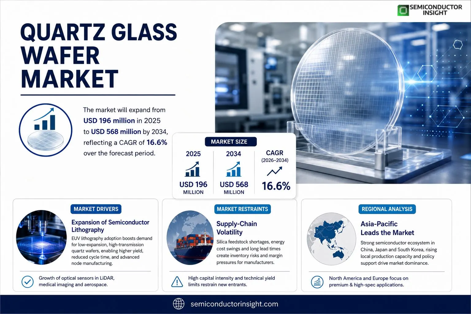
Quartz Glass Wafer market size was valued at USD 196 million in 2025. The market will expand from USD 196 million in 2025 to USD 568 million by 2034, reflecting a CAGR of 16.6 % over the forecast period.
Quartz glass wafers are wafer‑level substrates fabricated from high‑purity synthetic quartz or fused silica through precise slicing, double‑side grinding and polishing, thorough cleaning and semiconductor‑grade inspection. They replace conventional glassand occasionally ceramic or silicon carriersin environments demanding high temperature tolerance, ultraviolet resistance, high frequency operation and ultra‑clean conditions, thereby mitigating thermal expansion mismatch, limited optical transmission, contamination risk and insufficient electrical insulation reliability.Growth stems from heightened capital allocation toward advanced packaging and photonics, broader adoption of wafer‑level optics in 3D sensing and MEMS devices, and increasing requirements for low‑impurity, low‑birefringence substrates in biochip applications. Suppliers such as Corning, Shin‑Etsu and emerging Chinese manufacturers are extending product portfolios toward larger diameters (12 inch), ultra‑thin formats and microstructured processingtrends that improve pricing power and margin potential across multiple end markets.
MARKET DRIVERS
Expansion of Semiconductor Lithography
The shift toward extreme‑ultraviolet (EUV) lithography has forced fabs to seek substrates with superior transmission and low thermal expansion. Quartz glass wafers meet these specifications, prompting equipment manufacturers to standardize them across 300 mm production lines. This alignment reduces cycle time and enhances yield, making the material a logical choice for next‑generation node adoption.
Growth of Optical Sensor Applications
Automotive lidar, medical imaging, and aerospace telemetry increasingly rely on high‑purity quartz to achieve minimal signal loss. As OEMs integrate more sensors per vehicle or satellite, the aggregate demand for wafer‑scale quartz components rises sharply. Manufacturers benefit from economies of scale, translating into competitive pricing for downstream users.
➤ Industry analysts note that the convergence of advanced lithography and sensor integration creates a feedback loop, reinforcing the need for larger, defect‑free quartz glass wafers.
Beyond technology, regional policy incentives in East Asia and North America are channeling capital into clean‑room upgrades. These investments often require compliance with stricter substrate quality criteria, indirectly boosting orders for premium quartz glass wafer grades.
MARKET CHALLENGES
Supply‑Chain Volatility
Silica feedstock is subject to geopolitical constraints and fluctuating energy costs, which ripple through the wafer production chain. When raw material prices spike, manufacturers face margin compression, forcing some to delay capacity expansions. Strategic inventory management becomes essential, yet difficult in a market where lead times can exceed six months.
Other Challenges
Technical Yield Limitations
Achieving sub‑nanometer surface flatness on 200 mm and larger wafers demands ultra‑clean environments. Even minor particle contamination can render a batch unusable, inflating scrap rates. Companies that lack advanced polishing and inspection tooling experience higher per‑unit costs, reducing competitiveness.
MARKET RESTRAINTS
Capital Intensity of New Facilities
Establishing a dedicated quartz glass wafer line entails multi‑hundred‑million‑dollar outlays for furnaces, annealing chambers, and precision metrology. Smaller players often lack the financial bandwidth to enter the market, leading to a concentration of supply among a few large incumbents. This concentration can limit price flexibility and slow the diffusion of innovative wafer formats.
MARKET OPPORTUNITIES
Customization for Emerging Photonics
Photonics foundries are exploring heterogeneous integration that pairs silicon photonic circuits with quartz substrates to exploit quartz’s low loss at visible wavelengths. Tailored doping profiles and surface coatings represent a niche yet high‑margin segment. Early adopters that develop application‑specific quartz wafer offerings can capture premium pricing and lock in long‑term contracts.
Quartz Glass Wafer Market Trends
Shift Toward High‑Specification Substrates
Quartz Glass Wafer Market moved beyond a niche for heat‑resistant glass and now underpins performance‑critical layers in photomasks, wafer‑level optics, MEMS and advanced RF packaging. Customers are no longer satisfied with basic transmission or thermal resistance; they demand tight control of thickness‑variation, bow, surface roughness and metal impurity levels. This heightened specification regime has pushed manufacturers to integrate slicing, double‑side grinding, polishing and defect‑control into a single, highly automated value chain. Companies that can guarantee 4‑inch to 12‑inch formats with sub‑micron TTV and ultra‑thin, via‑enabled structures are able to command premium pricing, especially as the industry folds advanced packaging and 3‑D sensing into the same wafer footprint. The result is a market where volume growth is accompanied by a parallel rise in average selling price for premium grades.
Other Trends
Regional Supply‑Chain Realignment
Japanese firms retain leadership in synthetic quartz purity and ultra‑high‑grade HPFS material, while U.S. and European players have built reputation for precision processing and application‑specific customization. Chinese manufacturers are closing the gap by expanding large‑diameter, thin‑wafer lines and offering rapid prototyping for local semiconductor fabs. Policy programmes such as CHIPS for America, the European Chips Act and Chinese industrial subsidies have intensified domestic sourcing, creating a more regionally balanced supply landscape. Buyers are increasingly qualifying domestic suppliers that can meet the same defect‑density targets previously satisfied only by established Japanese sources, thereby reshaping long‑standing trade flows.
Emergence of Multi‑Application Platforms
Historically, quartz wafers served a single optical function, but today the same substrate family is being leveraged across photomask, microfluidic biochips, TGV interposers and laser optics. This convergence is driven by the material’s combination of low thermal expansion, high flatness and ability to support micro‑structuring. As design houses integrate several of these functions onto a single wafer, the demand signal becomes less volatile and more strategic. Suppliers that can provide a portfolio ranging from JGS1 deep‑UV to JGS3 infrared grades, along with custom thickness bands (ultra‑thin to thick), are positioned to capture a larger share of downstream spend. The strategic implication for investors is clear: companies that blend material science expertise with end‑to‑end processing and close customer collaboration will reap both higher margins and longer‑term contracts.
COMPETITIVE LANDSCAPEKey Industry Players
Quartz Glass Wafer Market: Competitive Overview 2025‑2034
Corning dominates the premium fused‑silica segment, leveraging its HPFS line to supply wafer‑level optics and 3‑D sensing. Its extensive clean‑room infrastructure and long‑standing relationships with leading semiconductor assemblers allow the company to command higher margins on 12‑inch and ultra‑thin formats. Japanese firms such as Shin‑Etsu and Asahi Glass retain control of the highest‑purity synthetic quartz feedstock, which translates into a defensible edge for photomask and deep‑UV applications. Meanwhile, European players like Plan Optik and Coresix focus on precision grinding and metrology services, positioning themselves as one‑stop solutions for customers who require tight TTV and low defect density. The overall structure resembles a concentrated core of material‑grade specialists flanked by a growing cohort of processors that add value through customization, rapid prototyping, and application‑specific grading.Beyond the tier‑one group, a heterogeneous set of niche manufacturers has emerged across Asia and North America. Companies such as Swift Glass, Sydor Optics, and Zhejiang Lante Optics excel in mid‑size diameters and cost‑effective thin‑wafer production, often securing regional contracts with MEMS and microfluidic developers. Chinese outfitsincluding D&X Co., WAFERFAB KOREA, and Hubei Feilihua Quartz Glassare accelerating capacity expansion, narrowing the gap in large‑diameter, low‑TTV capability through aggressive investment and localized supply chains. Smaller specialists like PHOENIX Inc., CQT Group, and YOFC Quartz Technology add depth by targeting emerging segments such as TGV advanced packaging and high‑frequency RF modules, thereby enriching the competitive fabric of the market.
List of Key Quartz Glass Wafer Companies Profiled
- Corning Inc.
- Shin‑Etsu Chemical Co., Ltd.
- Asahi Glass Co.
- OHARA Corp.
- Plan Optik AG
- Swift Glass
- Coresix Precision Glass
- Sydor Optics
- Zhejiang Lante Optics
- D&X Co., Ltd.
- WAFERFAB KOREA
- PHOENIX Inc.
- Hubei Feilihua Quartz Glass Co., Ltd.
- CQT Group
- YOFC Quartz Technology (Wuhan) Company Limited
Segment Analysis:
| Segment Category | Sub-Segments | Key Insights |
| By Type |
|
High‑purity synthetic quartz wafers
|
| By Application |
|
Wafer‑level optics & advanced packaging
|
| By End User |
|
Semiconductor & optical equipment sectors
|
| By Material Grade |
|
High‑performance grades (JGS1, HPFS)
|
| By Thickness |
|
Ultra‑thin and large‑diameter formats
|
Regional Analysis: Quartz Glass Wafer Market
Asia‑Pacific
Regional players have woven raw‑material sourcing, crucible production, and wafer finishing into a single logistical loop, curbing inventory buffers and enhancing responsiveness to specification shifts.
Joint research centers financed by governments and industry consortia accelerate breakthroughs in low‑thermal‑expansion glass formulations, aligning material performance with next‑generation lithography demands.
Energy‑recovery furnaces and water‑recycling loops have been adopted at scale, slashing operational expenditures while meeting tightening environmental standards across the region.
Universities and technical institutes are tailoring curricula to the nuances of quartz glass processing, ensuring a pipeline of engineers versed in both material science and precision manufacturing.
North America
The North American market leans heavily on legacy equipment manufacturers that have diversified into quartz glass production to serve aerospace and defense customers. Recent policy shifts encouraging domestic sourcing of high‑purity substrates have nudged incumbents to upgrade furnace capacity and invest in automated inspection. However, the region grapples with higher labor costs and stricter environmental permitting, prompting firms to explore modular production units that can be situated near end‑users, thereby reducing transportation overhead and complying with local emission limits. The strategic focus here is on premium‑grade wafers for quantum‑computing prototypes, where performance outweighs price considerations.
Europe
European players capitalize on a dense network of precision optics firms, especially in Germany and the Netherlands, where the demand for ultra‑stable quartz components in laser research remains robust. The continent’s regulatory framework drives manufacturers toward closed‑loop melt processes that recycle silica and minimize waste. Collaborative clusters, often anchored by research institutes, are experimenting with alloyed quartz to push thermal‑expansion limits, a move poised to open niche markets in space‑grade instrumentation. While the overall volume is modest compared with Asia‑Pacific, the emphasis on high‑value, low‑volume orders sustains profitability.
South America
In South America, the market is still emergent, anchored primarily by a handful of petrochemical off‑take agreements that supply silica feedstock. Local firms are gradually upgrading their annealing ovens to meet the stricter surface‑flatness criteria demanded by regional telecom upgrades. Investment is being channeled into joint ventures with Asian manufacturers, allowing technology transfer without the capital outlay of building full‑scale plants. The main business implication is the need to balance cost‑sensitivity with the aspiration to enter higher‑margin segments such as medical imaging.
Middle East & Africa
The Middle East & Africa region presents a mixed landscape where oil‑rich economies fund diversification projects that include advanced materials manufacturing. Pilot lines for quartz glass wafer fabrication have been inaugurated in the United Arab Emirates, targeting the burgeoning solar‑energy sector that requires durable, high‑temperature windows. Meanwhile, African nations are still at the stage of importing finished wafers, but governmental industrial‑park incentives hint at future local assembly capabilities. Companies eyeing this market must navigate fluctuating demand cycles while positioning themselves as preferred suppliers for emerging renewable‑energy infrastructure.
Report Scope
This market research report provides a comprehensive analysis of the Quartz Glass Wafer Market , covering the forecast period 2026–2034. It offers detailed insights into market dynamics, technological advancements, competitive landscape, and key trends shaping the industry.
Key focus areas of the report include:
- Market Overview: The report begins with an overview outlining its current market scenario, key growth indicators, and industry transformation drivers. It discusses macroeconomic factors, demand–supply balance, regulatory landscape, and the strategic role of semiconductors in powering advancements across industries such as automotive, telecommunications, consumer electronics, and industrial automation.
- Market Size & Forecast: Historical data and future projections for revenue, unit shipments, and market value across major regions and segments.
- Segmentation Analysis: Detailed breakdown by product type, technology, application, and end-user industry to identify high-growth segments and investment opportunities.
- Regional Insights: Insights into market performance across North America, Europe, Asia-Pacific, Latin America, and the Middle East & Africa, including country-level analysis where relevant.
- Competitive Landscape: Profiles of leading market participants, including their product offerings, R&D focus, manufacturing capacity, pricing strategies, and recent developments such as mergers, acquisitions, and partnerships.
- Technology Trends & Innovation: Assessment of emerging technologies, integration of AI/IoT, semiconductor design trends, fabrication techniques, and evolving industry standards.
- Market Drivers & Restraints: Evaluation of factors driving market growth along with challenges, supply chain constraints, regulatory issues, and market-entry barriers.
- Stakeholder Insights: Insights for component suppliers, OEMs, system integrators, investors, and policymakers regarding the evolving ecosystem and strategic opportunities.
Primary and secondary research methods are employed, including interviews with industry experts, data from verified sources, and real-time market intelligence to ensure the accuracy and reliability of the insights presented.
FREQUENTLY ASKED QUESTIONS:
What is the current market size of Quartz Glass Wafer Market?
-> Quartz Glass Wafer Market was valued at USD 196 million in 2025 and is expected to reach USD 568 million by 2034, growing at a CAGR of 16.6% over the forecast period.
Which key companies operate in Quartz Glass Wafer Market?
-> Key players include Asahi Glass Co, Corning, Plan Optik AG, Swift Glass, Coresix Precision Glass, Sydor Optics, Prazisions Glas & Optik, Valley Design, Zhejiang Lante Optics, Ohara, Shin-Etsu Chemical Co., Ltd., D&X Co., Ltd., WAFERFAB KOREA, PHOENIX Inc., Hubei Feilihua Quartz Glass Co., Ltd., CQT Group, HELIOS NEW MATERIALS LIMITED, YOFC Quartz Technology (Wuhan) Company Limited, Shanghai Xinkehui New Material Co., Ltd., JXT Technology Co.,Ltd.
What are the key growth drivers?
-> Key growth drivers include expanding applications in wafer‑level optics, 3D sensing, MEMS, microfluidics, biochips, RF devices, and advanced packaging; increasing demand for high‑purity, low‑impurity substrates; and supportive policies such as CHIPS for America, the National Advanced Packaging Manufacturing Program, and the European Chips Act.
Which region dominates the market?
-> Asia‑Pacific is the dominant and fastest‑growing region, driven by strong semiconductor manufacturing bases in China, Japan, and South Korea, as well as rapid localization of quartz wafer production.
What are the emerging trends?
-> Emerging trends include development of ultra‑thin and large‑diameter wafers with low TTV, micro‑structured and via‑enabled processing, and the shift toward high‑specification grades (e.g., JGS1, JGS2, HPFS) to enable next‑generation photonic and electronic devices.
Get Sample Report PDF for Exclusive Insights
Report Sample Includes
- Table of Contents
- List of Tables & Figures
- Charts, Research Methodology, and more...
 Download Sample Report PDF