Photomask Inspection Machine Market Insights
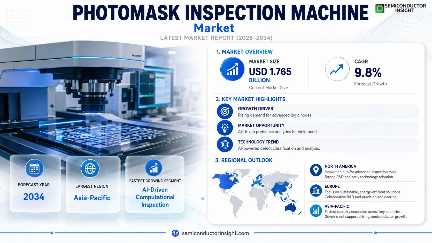
Photomask Inspection Machine market size was valued at USD 1.765 billion in 2026 and reaches USD 4.10 billion by 2034, reflecting an average annual growth rate of approximately 9.8% over the period.
Photomask Inspection Machine examines pattern defects and foreign particles on photomasks used in semiconductor fabrication. It serves semiconductor fabs, captive mask shops, and mask manufacturers by providing routine inspections of incoming masks and continuous monitoring throughout device production cycles. Typical unit prices run into several million dollars, while industry gross margins generally fall between 40 % and 60 %. Upstream components comprise precision optics, electron or ion beam subsystems, high‑stability stages, vibration isolation modules, high‑sensitivity detectors and industrial‑grade computing hardware together with software for image reconstruction, defect classification and workflow integration.
MARKET DRIVERS
Rising Demand for Advanced Logic Nodes
Manufacturers pushing sub‑10 nm processes require defect‑free photomasks to maintain yield. As pattern densities climb, even microscopic imperfections can cause multi‑layer failures. Inspection machines that combine high‑resolution imaging with AI‑assisted classification are becoming indispensable, prompting customers to upgrade equipment faster than in previous generations.
Increasing Chip Complexity and 3D Integration
Emergence of heterogeneous integration, such as chip‑on‑wafer and wafer‑level packaging, adds new layers of scrutiny to mask quality. The need to verify alignment marks across disparate materials forces suppliers to offer broader inspection windows and multi‑modal analysis. Companies that can certify mask integrity for these advanced packages are gaining market traction.
➤ “Customers are willing to pay a premium for tools that reduce re‑work cycles, because each mask defect can cost millions in downstream wafer processing.”
Overall, the cost‑benefit calculus for high‑precision inspection is shifting in favor of capital expenditures, as the penalty for a defective mask now outweighs the investment in next‑generation equipment.
MARKET CHALLENGES
Escalating Capital Outlay
State‑of‑the‑art inspection platforms command price tags exceeding $10 million, a barrier for mid‑size fabs that operate on thin margins. The upfront financial commitment creates hesitation, especially in regions where government subsidies for semiconductor infrastructure are still evolving.
Other Challenges
Skill Shortage
Operating and maintaining these sophisticated systems demands specialized training. The limited pool of engineers familiar with both optical metrology and machine learning algorithms slows adoption rates and raises ongoing service costs.
MARKET RESTRAINTS
Stringent Qualification Standards
Qualification protocols such as ISO‑26262 for safety‑critical devices impose exhaustive validation cycles. Each new inspection tool must undergo prolonged certification, which can defer market entry by several quarters.Regulatory scrutiny also extends to data privacy, as defect data is increasingly treated as proprietary IP. Vendors must implement robust cybersecurity measures, adding another layer of cost and complexity.Finally, the limited interchangeability of mask formats across equipment families means that fabs often lock into a single supplier ecosystem, reducing flexibility and dampening competitive pricing dynamics.
MARKET OPPORTUNITIES
AI‑Driven Predictive Analytics
Integrating real‑time defect prediction models enables fabs to pre‑emptively adjust lithography parameters, cutting downstream re‑work. Vendors that embed these analytics directly into inspection hardware can differentiate their offering and command higher margins.
Emerging Geographic Hubs
Investment waves in Southeast Asia and Eastern Europe are establishing new semiconductor fabs. These regions present a relatively untapped customer base for Photomask Inspection Machine Market, especially for modular, upgradable platforms that align with phased capacity expansions.Service‑oriented business modelssuch as equipment‑as‑a‑service (EaaS) and shared‑facility inspection labsaddress the barrier of high capital cost while delivering continuous technology refreshes, opening revenue streams beyond traditional sales.
Photomask Inspection Machine Market Trends
Shift Toward Sub‑Nanometer Accuracy
Photomask Inspection Machine Market is entering a phase where the tolerances required for mask defect detection are shrinking to the sub‑nanometer scale. This evolution mirrors the semiconductor industry’s push toward extreme ultraviolet (EUV) lithography, where even minute particles can jeopardize chip yield. Manufacturers are allocating resources to hybrid inspection architectures that combine deep‑ultraviolet (DUV) optics, electron‑beam re‑inspection, and advanced computational algorithms. The result is a tighter feedback loop between mask fabrication and wafer performance, allowing fabs to reduce scrap rates without sacrificing throughput. Suppliers that can embed high‑sensitivity detectors within vibration‑isolated stages gain a competitive edge, as their systems become indispensable for qualifying next‑generation reticles.
Other Trends
Integration of AI‑Driven Defect Classification
Artificial‑intelligence models are now being trained on millions of defect images, enabling real‑time classification that surpasses traditional rule‑based methods. By correlating defect signatures with process parameters, AI layers help operators prioritize remediation actions, which in turn shortens cycle time for mask repair. Vendors that package this intelligence as a service differentiate themselves from pure hardware providers, turning the inspection platform into a data‑rich hub that feeds predictive yield tools across the fab floor. This shift reduces the reliance on manual expert interpretation and creates new avenues for software licensing revenue.
Service‑Centric Revenue Models
Beyond the upfront capital outlay, Photomask Inspection Machine Market is seeing a rise in long‑term service contracts that bundle calibration, software updates, and spare‑part logistics. These agreements stabilize cash flow for equipment makers and give customers assurance that performance will keep pace with evolving mask designs. The recurring nature of such contracts also incentivizes manufacturers to invest in modular upgrades, ensuring that a single platform can adapt to both DUV and EUV inspection pathways over its lifespan. Consequently, the industry is moving from a transactional sales approach toward a partnership model that aligns equipment reliability with the fab’s yield objectives.
COMPETITIVE LANDSCAPEKey Industry Players
Photomask Inspection Machine Market: Competitive Overview
The market is dominated by a handful of suppliers that have combined deep expertise in precision optics, high‑stability mechanics, and semiconductor‑grade software. KLA leads the segment with its next‑generation EUV and DUV inspection platforms, leveraging a large installed base in leading fabs and a robust service network that monetizes recurring revenue through calibration and software upgrades. Applied Materials follows closely, differentiating its offering through integrated metrology suites that couple mask inspection with wafer‑level defect correlation, a capability that appeals to manufacturers seeking end‑to‑end yield assurance. Lasertec and Carl Zeiss occupy niche leadership in electron‑beam re‑inspection and ultra‑high‑resolution optical systems, respectively, positioning themselves as technology specialists for customers tackling sub‑nanometer defect detection as process nodes shrink.Beyond the marquee names, a constellation of mid‑size firms fuels innovation in specific sub‑domains. NuFlare Technology focuses on AI‑enhanced defect classification, while Advantest provides cost‑effective inspection solutions for captive mask shops. MueTec, LAZIN, VPtek, Yuweitek, TENYUM, and SUSS MicroTec each address particular workflow requirements, such as high‑throughput wafer‑level review or compact systems for fab‑floor deployment. These players often partner with larger OEMs or offer proprietary software layers that integrate inspection data into predictive yield models, thereby extending their influence beyond the hardware scope and shaping the overall value chain.
List of Key Photomask Inspection Machine Companies Profiled
- KLA Corp.
- Applied Materials
- Lasertec
- Carl Zeiss
- NuFlare Technology
- Advantest
- MueTec
- LAZIN
- VPtek
- Yuweitek
- TENYUM
- SUSS MicroTec
- Nikon Corporation
Segment Analysis:
| Segment Category | Sub-Segments | Key Insights |
| By Type |
|
Mask Pattern Defect Detection drives market interest because it directly supports yield optimization in advanced lithography.
|
| By Application |
|
Semiconductor Fabrication remains the cornerstone application as mask inspection directly influences device yield.
|
| By End User |
|
Semiconductor Fabs prioritize inspection solutions that embed seamlessly into their production flow.
|
| By Technology |
|
AI‑Driven Computational is emerging as a strategic differentiator because it enhances defect detection without proportional hardware cost increases.
|
| By Service Model |
|
Integrated Software & Service resonates with customers seeking end‑to‑end quality assurance.
|
Regional Analysis: Photomask Inspection Machine Market
Leading fabs are integrating machine‑learning models that differentiate subtle pattern variations, allowing operators to prioritize critical defects early in the process. This capability reduces re‑work cycles and aligns inspection output with tighter design tolerances.
Recent geopolitical shifts have encouraged manufacturers to source key components domestically, shortening lead times for high‑value inspection equipment and mitigating exposure to cross‑border disruptions.
Federal agencies have issued detailed standards for photomask integrity, giving customers confidence that purchased systems comply with industry‑wide safety and performance benchmarks.
Silicon Valley and the Research Triangle foster a revolving door of talent between universities and equipment firms, accelerating the transition of prototype technologies into commercial inspection platforms.
Europe
European mask makers are capitalizing on a mature ecosystem that couples precision engineering with an emphasis on sustainability. Clients increasingly demand inspection tools that not only deliver high resolution but also operate with reduced energy footprints, prompting vendors to adopt modular designs that can be upgraded rather than replaced. Collaborative research programs across the EU encourage shared risk, enabling smaller players to access cutting‑edge optics without bearing the full cost of development. As a result, the market sees a steady stream of niche solutions tailored to advanced packaging applications.
Asia‑Pacific
The Asia‑Pacific region experiences a surge in capacity expansion as new fabs come online in China, Taiwan, and South Korea. Local governments offer incentives for technology transfer, nudging equipment manufacturers to establish regional R&D centers. This proximity shortens feedback loops, allowing rapid iteration of inspection algorithms that address the specific defect profiles encountered in high‑volume production. However, divergent standards across jurisdictions create a patchwork of compliance requirements, compelling vendors to adopt flexible software architectures.
South America
South American semiconductor activity remains modest, yet emerging investment in microelectronics hubs signals a gradual shift. Companies entering Photomask Inspection Machine Market are focusing on cost‑effective platforms that balance performance with affordability, catering to nascent manufacturers aiming to serve regional automotive and aerospace suppliers. Partnerships with North American distributors help bridge expertise gaps, while local training programs raise the skill level of technicians handling sophisticated inspection workflows.
Middle East & Africa
In the Middle East & Africa, market growth is anchored by government‑led initiatives to diversify economies beyond oil and minerals. Pilot projects in United Arab Emirates and South Africa explore photomask inspection as part of broader semiconductor value‑chain development. These early‑stage efforts prioritize flexible, scalable equipment that can be integrated into multipurpose fabrication lines. Although adoption rates are still low, the strategic emphasis on technology transfer indicates a long‑term appetite for advanced inspection capabilities.
Report Scope
This market research report provides a comprehensive analysis of Photomask Inspection Machine Market , covering the forecast period 2026–2034. It offers detailed insights into market dynamics, technological advancements, competitive landscape, and key trends shaping the industry.
Key focus areas of the report include:
- Market Overview: The report begins with an overview outlining its current market scenario, key growth indicators, and industry transformation drivers. It discusses macroeconomic factors, demand–supply balance, regulatory landscape, and the strategic role of semiconductors in powering advancements across industries such as automotive, telecommunications, consumer electronics, and industrial automation.
- Market Size & Forecast: Historical data and future projections for revenue, unit shipments, and market value across major regions and segments.
- Segmentation Analysis: Detailed breakdown by product type, technology, application, and end-user industry to identify high-growth segments and investment opportunities.
- Regional Insights: Insights into market performance across North America, Europe, Asia-Pacific, Latin America, and the Middle East & Africa, including country-level analysis where relevant.
- Competitive Landscape: Profiles of leading market participants, including their product offerings, R&D focus, manufacturing capacity, pricing strategies, and recent developments such as mergers, acquisitions, and partnerships.
- Technology Trends & Innovation: Assessment of emerging technologies, integration of AI/IoT, semiconductor design trends, fabrication techniques, and evolving industry standards.
- Market Drivers & Restraints: Evaluation of factors driving market growth along with challenges, supply chain constraints, regulatory issues, and market-entry barriers.
- Stakeholder Insights: Insights for component suppliers, OEMs, system integrators, investors, and policymakers regarding the evolving ecosystem and strategic opportunities.
Primary and secondary research methods are employed, including interviews with industry experts, data from verified sources, and real-time market intelligence to ensure the accuracy and reliability of the insights presented.
FREQUENTLY ASKED QUESTIONS:
What is the current market size of Photomask Inspection Machine Market?
-> Photomask Inspection Machine Market was valued at USD 1,765 million in 2026 and is expected to reach USD 3,400 million by 2034 at a CAGR of 9.9% during the forecast period.
Which key companies operate in Photomask Inspection Machine Market?
-> Key players include Lasertec, KLA, Applied Materials, NuFlare Technology, Advantest, Carl Zeiss, MueTec, LAZIN, VPtek, Yuweitek, TENYUM.
What are the key growth drivers?
-> Key growth drivers include advancement to higher semiconductor process nodes, adoption of extreme ultraviolet (EUV) lithography, demand for sub‑nanometer defect detection, and the integration of AI‑driven computational inspection technologies.
Which region dominates the market?
-> Asia-Pacific leads the market, driven by a high concentration of semiconductor fabs and mask manufacturers, while Europe and North America also hold significant shares.
What are the emerging trends?
-> Emerging trends include AI‑enabled defect classification, EUV optical inspection, electron‑beam re‑inspection, and fully integrated quality‑control solutions linked to predictive yield management systems.

Get Sample Report PDF for Exclusive Insights
Report Sample Includes
- Table of Contents
- List of Tables & Figures
- Charts, Research Methodology, and more...
 Download Sample Report PDF