Key Statistics
Key Takeaways
- Quartz photomasks are the dominant source-defined type because advanced semiconductor patterning requires superior dimensional stability, optical performance and compatibility with high-resolution writing and inspection.
- Semiconductor chip manufacturing is the most demanding and commercially important application, while display, touch and circuit-board production sustain high-volume mature-resolution mask demand.
- EUV and High-NA EUV are the fastest value-growth areas because reflective mask stacks, blank quality, inspection and defect repair become more complex as logic nodes move beyond current EUV generations.
- Asia Pacific is the largest and fastest-growing region through its concentration of foundries, memory fabs, display manufacturers and mask suppliers in Japan, Taiwan, South Korea and China.
- Mask-writing and inspection capital intensity, advanced blank concentration and long leading-edge qualification restrain new entry even as mature-node masks remain price competitive.
Photomask for Lithography Market Overview
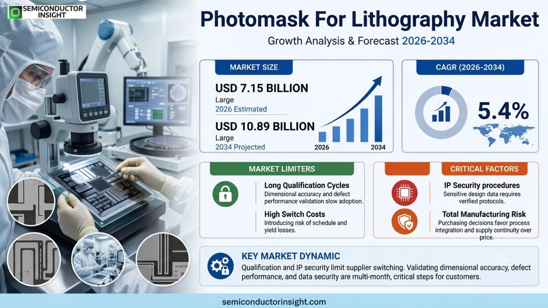
Photomask For Lithography Market was valued at USD 6.78 billion in 2025 and is projected to reach USD 10.89 billion by 2034, representing a 5.4% CAGR during 2026–2034. The 2026 estimated market size is USD 7.15 billion. Asia Pacific is the largest and fastest-growing market in 2025, supported by the concentration of wafer fabrication, display production, advanced photomask suppliers and EUV/DUV manufacturing ecosystems.
A photomask is the precision master pattern used by lithography equipment to transfer circuit, display or other micro-scale structures onto a coated substrate. Conventional DUV masks use patterned absorber layers on quartz or other transparent substrates, while EUV masks use reflective multilayer structures. A single advanced semiconductor design can require many masks, making reticle quality, turnaround and defect control central to wafer yield and time to market.
Photomasks are economically unusual because a customer purchases a small number of physical units that control the patterning of very large wafer volumes. A defect, data error or delayed mask can interrupt production worth far more than the mask itself. This supports premium pricing for leading-edge capability, fast cycle time, repair, secure data handling and proven defect inspection rather than competition on substrate cost alone.
Technology scaling changes the mix of value. Mature-node DUV and display masks remain important for automotive, industrial, analog and consumer electronics, while EUV and High-NA development raise requirements for mask blanks, multilayers, absorber structures, pellicles and inspection. DNP and HOYA capacity initiatives show suppliers investing ahead of sub-2-nm and High-NA production ramps.
Segment Analysis: By Type
The source page segments the market into Quartz Photomask, Soda-Lime Photomask and Other Materials. Quartz Photomask is explicitly identified as dominant because its thermal stability and optical properties support tighter patterning. Soda-lime remains relevant in cost-sensitive display and mature applications, while other materials include specialized substrates and reflective EUV structures. This matters commercially because process qualification, integration effort, supply continuity, engineering support and total manufacturing risk often influence purchasing decisions as strongly as component price, so suppliers that solve deployment constraints can defend approved positions even when technically similar alternatives are available.
| Type | Technical / purchasing role | Market position |
|---|---|---|
| Quartz Photomask | Quartz substrates provide high dimensional stability, low thermal expansion and suitable optical characteristics for demanding DUV lithography. Advanced masks add chrome, phase-shift or other patterned layers and require high-resolution writing, inspection and repair, making substrate flatness and defect quality fundamental to the manufacturing process. This matters commercially because process qualification, integration effort, supply continuity, engineering support and total manufacturing risk often influence purchasing decisions as strongly as component price, so suppliers that solve deployment constraints can defend approved positions even when technically similar alternatives are available. | Dominant type. The source page identifies quartz photomasks as the leading format. Their advantage increases with tighter overlay and critical-dimension control because mask distortion affects the transferred wafer pattern. Suppliers compete through blank quality, writer capability, OPC handling, inspection and turnaround rather than quartz cost alone. This matters commercially because process qualification, integration effort, supply continuity, engineering support and total manufacturing risk often influence purchasing decisions as strongly as component price, so suppliers that solve deployment constraints can defend approved positions even when technically similar alternatives are available. |
| Soda-Lime Photomask | Soda-lime glass masks provide a lower-cost substrate for less demanding resolution and dimensional-stability requirements. They are associated with mature display, touch, PCB and prototype applications where the cost premium of high-grade quartz would not generate a proportionate yield or resolution benefit. This matters commercially because process qualification, integration effort, supply continuity, engineering support and total manufacturing risk often influence purchasing decisions as strongly as component price, so suppliers that solve deployment constraints can defend approved positions even when technically similar alternatives are available. | A mature, price-sensitive segment that remains relevant outside leading-edge semiconductor lithography. Suppliers win through efficient writing, short turnaround and flexible size formats. Growth is slower than quartz and EUV-related masks, but the installed base of display, touch and circuit-board processes sustains recurring demand. This matters commercially because process qualification, integration effort, supply continuity, engineering support and total manufacturing risk often influence purchasing decisions as strongly as component price, so suppliers that solve deployment constraints can defend approved positions even when technically similar alternatives are available. |
| Other Materials | The source-defined category includes specialized substrates and reflective EUV mask structures that do not fit conventional transparent quartz or soda-lime classifications. EUV reticles depend on multilayer reflective stacks and specialized absorbers, making blank fabrication, surface quality and defect inspection different from transmissive mask production. This matters commercially because process qualification, integration effort, supply continuity, engineering support and total manufacturing risk often influence purchasing decisions as strongly as component price, so suppliers that solve deployment constraints can defend approved positions even when technically similar alternatives are available. | Fastest value-growth area through EUV-related structures. Advanced nodes require higher-value mask blanks and more complex inspection, repair and pellicle ecosystems. High-NA EUV extends this trajectory by tightening imaging requirements, so suppliers capable of next-generation blanks, multilayers and defect control can grow faster than the mature transparent-mask base. This matters commercially because process qualification, integration effort, supply continuity, engineering support and total manufacturing risk often influence purchasing decisions as strongly as component price, so suppliers that solve deployment constraints can defend approved positions even when technically similar alternatives are available. |
Technology segmentation: DUV, EUV and High-NA
DUV remains indispensable because even leading-edge chips use a mix of EUV and DUV layers, while mature-node semiconductor and display production remains DUV based. EUV adds reflective masks and new defect modes, increasing mask value and inspection complexity. High-NA EUV, with 0.55 numerical aperture, pushes the ecosystem further by changing imaging conditions and requiring advances in blank flatness, absorber design, pellicles and defect management.
Segment Analysis: By Application
The source applications are Semiconductor Chip Manufacturing, Flat Panel Display Production, Touch Industry and Circuit Board Fabrication. Semiconductor chip manufacturing is the most demanding and highest-value application because advanced nodes require complex OPC, phase-shift and EUV masks with stringent defect control. Display, touch and PCB applications use larger or lower-resolution masks where throughput, panel size and cost per area matter more.
| Application | Demand characteristics |
|---|---|
| Semiconductor Chip Manufacturing | Largest and highest-value application. Logic, memory, analog, power and specialty devices use multiple photomasks to define process layers. Leading-edge designs increase data volume, writing time and inspection difficulty, while mature nodes require reliable mask replication and long-term archival support. Supplier turnaround directly affects tape-out schedules, wafer starts and engineering changes. This matters commercially because process qualification, integration effort, supply continuity, engineering support and total manufacturing risk often influence purchasing decisions as strongly as component price, so suppliers that solve deployment constraints can defend approved positions even when technically similar alternatives are available. |
| Flat Panel Display Production | Display masks pattern thin-film transistor arrays and color-filter or related structures across large substrates. Resolution is less extreme than advanced IC lithography, but mask dimensions are much larger and uniformity across the plate is critical. Suppliers compete through large-format writing capacity, dimensional control, defect repair and efficient production for LCD and OLED manufacturing. |
| Touch Industry | Touch sensors and related patterned conductors use photomasks for electrode and circuit structures. The application favors mature lithography where throughput, large-area uniformity and mask cost are key. Demand follows display and consumer-electronics manufacturing, and suppliers can serve using established writing and inspection tools without EUV capital intensity. This matters commercially because process qualification, integration effort, supply continuity, engineering support and total manufacturing risk often influence purchasing decisions as strongly as component price, so suppliers that solve deployment constraints can defend approved positions even when technically similar alternatives are available. |
| Circuit Board Fabrication | Printed circuit and advanced substrate production uses phototools or photomasks to define fine conductive patterns. The segment is cost and throughput sensitive, but finer lines in advanced packaging substrates can raise resolution requirements. Suppliers compete through fast data preparation, large-format capability and predictable reproduction across production sites. This matters commercially because process qualification, integration effort, supply continuity, engineering support and total manufacturing risk often influence purchasing decisions as strongly as component price, so suppliers that solve deployment constraints can defend approved positions even when technically similar alternatives are available. |
Regional Analysis
Asia Pacific leads because photomask demand follows wafer fabs, display factories and the specialist mask supply chain. North America is important for chip design, advanced logic R&D and fab localization; Europe influences technology through lithography equipment and specialty fabs. South America and Middle East & Africa remain smaller prototype and research markets dependent on imported reticles and international mask shops.
How does regional demand differ across the photomask for lithography market?
Regional economics differ according to whether a location designs chips, manufactures wafers, builds displays or supplies lithography technology. Asia combines all four at scale, creating the deepest mask market. North America generates high-value design revisions and domestic fab demand. Europe shapes advanced imaging requirements while supporting long-life specialty products. Emerging regions rely on prototype services, making logistics and engineering support primary competitive variables.
| Region | Position | Growth outlook | Demand profile | What decides supplier selection |
|---|---|---|---|---|
| Asia Pacific | Largest | Highest in market | Foundry, memory, display and mask-supply-chain led | Defect control, turnaround and node qualification |
| North America | Major established market | Strong | Chip design and fab localization led | Turnaround, IP security and repair capability |
| Europe | Major established market | Steady | Lithography equipment and specialty-fab led | Roadmap alignment and long-term supply |
| South America | Emerging | Selective | Research and import led | Prototype access and logistics |
| Middle East & Africa | Emerging | Selective | Design and research led | IP security and import reliability |
Competitive Landscape
The competitive structure combines large merchant photomask producers, closely aligned mask operations, mask-blank specialists and regional prototype suppliers. The source page profiles Photronics, Tekscend/Toppan, DNP, HOYA, SK-Electronics, Taiwan Mask, Compugraphics and others. Competitive advantage depends on writer and inspection capability, blank access, repair, turnaround, secure data handling and customer qualification at specific nodes.
Photronics is a major merchant supplier across integrated-circuit and display masks, using a multi-site network to serve regional customers. DNP and Tekscend bring deep Japanese patterning expertise and advanced-node relationships, while HOYA is important upstream in EUV mask blanks. This specialization means the value chain cannot be understood by ranking companies only on total mask revenue.
Leading-edge competition is capital intensive. Electron-beam writers, advanced inspection, repair and cleanroom infrastructure require significant investment, and EUV adds specialized blank and defect-control challenges. This creates a higher barrier than mature-node production, where regional suppliers can compete on cost and cycle time. The result is concentrated advanced capability alongside broader mature-node and display capacity.
Turnaround can be as important as mask price. A foundry or design house may need an engineering reticle quickly after silicon learning reveals a pattern issue. Suppliers with local data preparation, writer availability, repair and secure delivery can protect customer schedules. Once embedded in a customer’s process and design-data workflow, switching carries operational and IP risk.
Tier structure
| Competitive tier | Representative participants | How suppliers compete |
|---|---|---|
| Global advanced merchant mask leaders | Photronics; DNP; Tekscend Photomask | Compete through leading-edge writing and inspection, broad node coverage, regional manufacturing networks and deep customer qualification. Their advantage is the ability to support both high-value advanced masks and the larger DUV installed base with dependable turnaround and engineering services. This matters commercially because process qualification, integration effort, supply continuity, engineering support and total manufacturing risk often influence purchasing decisions as strongly as component price, so suppliers that solve deployment constraints can defend approved positions even when technically similar alternatives are available. |
| Mask blank & advanced materials specialists | HOYA and related high-purity substrate suppliers | Capture value upstream through substrate flatness, multilayer deposition, defect control and next-generation EUV blank capability. High-NA and future EUV generations increase their strategic importance because blank defects become harder to tolerate and mask makers depend on a limited set of qualified advanced sources. This matters commercially because process qualification, integration effort, supply continuity, engineering support and total manufacturing risk often influence purchasing decisions as strongly as component price, so suppliers that solve deployment constraints can defend approved positions even when technically similar alternatives are available. |
| Regional & specialty suppliers | SK-Electronics; Taiwan Mask; Compugraphics; QingVi; Newway; STARMASK; Nippon Filcon | Serve mature-node, display, prototype and regional semiconductor customers through cost, short cycle time, specialty sizes and local support. Moving toward advanced nodes requires heavy capital and qualification, so many focus on niches where rapid service and flexible production matter more than absolute resolution leadership. This matters commercially because process qualification, integration effort, supply continuity, engineering support and total manufacturing risk often influence purchasing decisions as strongly as component price, so suppliers that solve deployment constraints can defend approved positions even when technically similar alternatives are available. |
Key companies profiled
The source report profiles Photronics, Inc.; Toppan Photomask Co., Ltd. (Tekscend Photomask); Dai Nippon Printing Co., Ltd. (DNP); HOYA Corporation; SK-Electronics Co., Ltd.; LG Innotek; ShenZheng QingVi Photomask Limited; Taiwan Mask Corporation; Nippon Filcon Co., Ltd.; Compugraphics International Ltd.; Newway Photomask Co., Ltd.; STARMASK. The list mixes high-volume merchant photomask producers, advanced Japanese technology suppliers and regional specialty shops. A meaningful competitive assessment separates mask blank capability, advanced IC reticle writing, display masks, prototype service and regional manufacturing because total corporate scale does not reveal whether a supplier can meet a particular node, format, defect specification or turnaround requirement.
Photomask for Lithography Production Capacity Analysis
Production capacity is determined by mask-blank supply, high-resolution data preparation, electron-beam or laser writing time, resist and etch processing, inspection, repair and clean handling. The bottleneck changes by technology: mature masks are constrained mainly by writer utilization and turnaround, while leading-edge EUV capacity also depends on advanced blanks, specialized inspection, defect repair and qualification with demanding customers.
Mask writers are a central capital constraint because exposure time grows with pattern complexity and data volume. Advanced OPC and sub-resolution features increase shot count, while high-resolution e-beam tools are expensive and difficult to replace quickly. Capacity planning therefore considers writer count, average write time per mask, engineering rework and the mix of advanced versus mature orders.
EUV and High-NA capacity introduces an upstream blank bottleneck. Reflective multilayer blanks require extreme surface quality and low defect density before pattern writing. HOYA’s planned Singapore EUV mask-blank plant, with 42 billion yen initial investment and FY28 start target, shows suppliers adding dedicated capacity ahead of expected High-NA and advanced-node growth rather than relying on DUV infrastructure.
Inspection and repair can constrain output after writing. A completed mask must be measured for critical dimension, placement and defects, and advanced masks may require multiple inspection or correction cycles. Faster writing alone does not improve shipment capacity if inspection tools are saturated, so leading suppliers invest across the workflow and use data automation to shorten disposition time.
Photomask for Lithography Market Dynamics: Drivers, Restraints and Opportunities
Growth is driven by node scaling, EUV/High-NA adoption, increasing design complexity and continued mature-node wafer and display production. Restraints include writer and inspection capital intensity, concentrated advanced blank supply, escalating mask-set cost and long qualification. Opportunities center on High-NA-ready blanks and masks, faster turnaround, secure regional capacity, advanced repair and long-lifecycle services.
MARKET DRIVERS
Drivers Impact Analysis*
| Factor | Relative impact* | Commercial mechanism |
|---|---|---|
| EUV and High-NA adoption | High | Reflective masks, advanced blanks and tighter defect requirements increase value per mask. |
| More complex chip designs | High | Higher layer counts and OPC complexity raise writing and inspection content. |
| Fab capacity expansion | Medium-High | New fabs require development and production mask sets. |
| Mature-node and display continuity | Medium | Long-lived automotive, industrial and panel production sustains DUV demand. |
EUV and High-NA raise technical value per reticle
EUV masks use reflective multilayers and specialized absorbers rather than conventional transmissive architecture, creating new defect and inspection challenges. High-NA tightens imaging conditions further. DNP’s High-NA sample work and HOYA’s planned blank expansion indicate that suppliers expect advanced reticle value to grow as sub-2-nm and future nodes move toward production.
Chip complexity increases mask data and engineering content
Modern designs use aggressive optical proximity correction, sub-resolution assist features and many process layers. This increases data preparation, write time and inspection load even when the physical mask count changes modestly. Suppliers with fast computing, writer capacity and automated review can reduce cycle time and capture premium work from customers prioritizing time to first silicon.
Global fab expansion creates new mask qualification events
New logic, memory, power and specialty fabs need mask supply for process development and production. Localization in the United States, Japan and Europe adds demand outside traditional Asian clusters, while China expands mature and selected advanced capacity. Mask suppliers can win durable positions by establishing local service and qualification before high-volume manufacturing.
Mature-node products sustain a broad DUV base
Automotive, industrial, analog, power and connectivity devices remain on mature nodes because cost, voltage capability and long product life can matter more than maximum transistor density. These fabs continue to consume DUV mask sets and engineering revisions for many years, providing stable demand that balances higher-growth but concentrated EUV work. This matters commercially because process qualification, integration effort, supply continuity, engineering support and total manufacturing risk often influence purchasing decisions as strongly as component price, so suppliers that solve deployment constraints can defend approved positions even when technically similar alternatives are available.
MARKET RESTRAINTS
Restraints Impact Analysis*
| Factor | Relative impact* | Commercial mechanism |
|---|---|---|
| Advanced writer and inspection capital intensity | High | Leading-edge capacity requires expensive tools and specialized operation. |
| EUV blank concentration | High | A small supplier base can constrain advanced mask capacity. |
| Rising mask-set cost | Medium-High | Complex mask sets increase development expense. |
| Qualification and secure-data requirements | Medium | Customers restrict switching because reticles contain critical IP. |
Leading-edge mask capacity is expensive to create
A new advanced mask line requires high-resolution writers, metrology, inspection, repair and ultra-clean processing, not simply floor space. Tool lead times and specialized operator skills limit how quickly capacity can expand. This protects incumbents but can create cycle-time pressure when multiple leading-edge customers ramp and compete for the same advanced writer hours.
Advanced blank supply remains concentrated
EUV masks begin with specialized reflective blanks that must meet severe flatness and defect requirements. A defect present before pattern writing can make the finished reticle unusable, so mask shops rely on a limited set of qualified blank sources. Supply concentration raises strategic inventory needs and makes new blank-capacity investments important to the broader market.
Mask-set economics can constrain design iteration
Advanced masks are costly because writing, inspection and repair become more complex, and a full chip can require many reticles. Design teams balance an additional mask revision against schedule and budget. Higher reticle cost does not stop leading-edge development, but can encourage more simulation, multi-project wafers and disciplined tape-out practices before committing to physical masks.
Qualification and IP security limit supplier switching
A photomask contains sensitive design data and directly controls printed wafer patterns. Customers validate dimensional accuracy, defect performance, data-security procedures and logistics before trusting a new supplier. Even if another shop offers a lower price, switching can introduce schedule, yield and intellectual-property risk, making diversification slower than in less critical consumables. This matters commercially because process qualification, integration effort, supply continuity, engineering support and total manufacturing risk often influence purchasing decisions as strongly as component price, so suppliers that solve deployment constraints can defend approved positions even when technically similar alternatives are available.
MARKET OPPORTUNITIES
High-NA EUV mask and blank capability
High-NA lithography creates opportunities across mask blanks, absorber materials, patterning, inspection, pellicles and repair. Suppliers that qualify early with scanner, foundry and research partners can secure premium positions as sub-2-nm and future nodes scale. DNP sample supply and HOYA capacity investment show the ecosystem moving from research toward production readiness. This matters commercially because process qualification, integration effort, supply continuity, engineering support and total manufacturing risk often influence purchasing decisions as strongly as component price, so suppliers that solve deployment constraints can defend approved positions even when technically similar alternatives are available.
Regional mask capacity beside new fabs
Semiconductor localization creates demand for faster reticle turnaround outside traditional Asian centers. Building or expanding mask shops near new U.S., Japanese and European fabs can reduce logistics and accelerate engineering loops. The case is strongest for prototype and high-value production masks where a few days can influence an expensive fab ramp schedule.
Digital workflow and AI-assisted data preparation
Mask data volumes grow with OPC and complex patterning. Automation in fracturing, rule checking, inspection review and defect classification can shorten non-writing cycle time and increase effective equipment utilization. Suppliers combining software with writer capacity can improve turnaround without adding identical amounts of capital, creating a productivity-based advantage. This matters commercially because process qualification, integration effort, supply continuity, engineering support and total manufacturing risk often influence purchasing decisions as strongly as component price, so suppliers that solve deployment constraints can defend approved positions even when technically similar alternatives are available.
Long-lifecycle services for mature-node reticles
Automotive and industrial customers may need the same device family for a decade or longer. Mask suppliers can create recurring revenue through archival storage, certified remakes, cleaning, repair and controlled process migration when old equipment is retired. The value proposition is supply assurance and exact pattern reproducibility rather than leading-edge resolution. This matters commercially because process qualification, integration effort, supply continuity, engineering support and total manufacturing risk often influence purchasing decisions as strongly as component price, so suppliers that solve deployment constraints can defend approved positions even when technically similar alternatives are available.
Photomask for Lithography Supply Chain Analysis
Mask substrates & blanks
Upstream blank quality sets the floor for finished mask performance. Quartz requires dimensional stability and low defects; EUV blanks add controlled multilayer stacks and severe surface requirements. Suppliers such as HOYA invest heavily in advanced blank production because a mask shop cannot compensate for certain substrate defects after patterning begins. This matters commercially because process qualification, integration effort, supply continuity, engineering support and total manufacturing risk often influence purchasing decisions as strongly as component price, so suppliers that solve deployment constraints can defend approved positions even when technically similar alternatives are available.
Data preparation & mask writing
Design data is fractured, corrected and translated into writer formats before exposure. Advanced OPC generates large data sets and long write times, making computing efficiency and writer scheduling important capacity levers. Secure data handling is essential because mask files contain customer intellectual property before a physical reticle exists. This matters commercially because process qualification, integration effort, supply continuity, engineering support and total manufacturing risk often influence purchasing decisions as strongly as component price, so suppliers that solve deployment constraints can defend approved positions even when technically similar alternatives are available.
Process, inspect & repair
After writing, the mask passes through resist development, pattern transfer and inspection. Defects or dimensional excursions may require repair or a complete rewrite. Advanced EUV masks demand specialized inspection, so metrology and repair capacity can become as important as writer availability in shipment cycle time and yield. This matters commercially because process qualification, integration effort, supply continuity, engineering support and total manufacturing risk often influence purchasing decisions as strongly as component price, so suppliers that solve deployment constraints can defend approved positions even when technically similar alternatives are available.
Fab use, cleaning & lifecycle support
Fabs mount photomasks in lithography scanners under strict handling protocols and may use pellicles. Suppliers support cleaning, repair, archival data and remakes throughout a device’s production life. Rapid response is valuable because a damaged reticle can stop exposures on a high-utilization lithography tool and delay wafer output. This matters commercially because process qualification, integration effort, supply continuity, engineering support and total manufacturing risk often influence purchasing decisions as strongly as component price, so suppliers that solve deployment constraints can defend approved positions even when technically similar alternatives are available.
Recent Developments in the Photomask for Lithography Market
Recent primary-source developments concentrate on High-NA EUV readiness and new advanced mask-blank capacity. DNP is linking investment to Rapidus’s 2 nm plans, HOYA is planning a Singapore EUV blank expansion, and ASML continues to advance High-NA scanners. These moves show the leading edge of photomask value growth shifting toward specialized reticle materials and defect control.
DNP announced investment to support mass production of EUV photomasks associated with Rapidus’s planned 2 nm manufacturing. The move links mask capacity directly to a future leading-edge fab ramp and highlights the value of early supplier qualification because reticle technology and production readiness must be established before high-volume wafer manufacturing begins.
HOYA’s Integrated Report 2026 says the company plans a new EUV mask-blank plant adjacent to its existing Singapore facility, with initial investment of 42 billion yen and planned operation in FY28. The project responds to expected growth in EUV mask blanks and prepares capacity for High-NA and future lithography roadmaps. This matters commercially because process qualification, integration effort, supply continuity, engineering support and total manufacturing risk often influence purchasing decisions as strongly as component price, so suppliers that solve deployment constraints can defend approved positions even when technically similar alternatives are available.
DNP announced sample supply of photomasks for High-NA EUV lithography aimed at semiconductor processes beyond 2 nm. Early sample availability matters because foundries and research programs need reticles to characterize scanner imaging, process windows and defect behavior before commercial node ramps, giving qualified suppliers a first-mover advantage. This matters commercially because process qualification, integration effort, supply continuity, engineering support and total manufacturing risk often influence purchasing decisions as strongly as component price, so suppliers that solve deployment constraints can defend approved positions even when technically similar alternatives are available.
REPORT SCOPE & SEGMENTATION
The report scope preserves the source page’s type and application segmentation and its additional end-user, technology and resolution views while using the published USD 6,783 million 2025 and USD 10,889 million 2034 market-size anchors. Those anchors imply a 5.4% annual growth rate, which replaces the source page’s conflicting printed 7.1% CAGR in the standardized 2026–2034 series.
| Report attribute | Coverage |
|---|---|
| Market | Photomask for Lithography |
| Base year | 2025 |
| Estimated year | 2026 |
| Forecast period | 2026–2034 |
| 2025 market size | USD 6.78 billion |
| 2034 forecast size | USD 10.89 billion |
| CAGR | 5.4% during 2026–2034 |
| Largest market in 2025 | Asia Pacific |
| By Type | Quartz Photomask; Soda-Lime Photomask; Other Materials |
| By Application | Semiconductor Chip Manufacturing; Flat Panel Display Production; Touch Industry; Circuit Board Fabrication |
| Additional segmentation | By End User: Chipmakers; Display Manufacturers; Consumer-Electronics Assemblers. By Technology: EUV Mask; DUV Mask; Hybrid/Multilayer. By Resolution: Advanced Node below 7 nm; Mature 7 nm and above; Specialty High-Resolution |
| Regions | North America; Europe; Asia Pacific; South America; Middle East & Africa |
| Companies profiled | Photronics, Inc.; Toppan Photomask Co., Ltd. (Tekscend Photomask); Dai Nippon Printing Co., Ltd. (DNP); HOYA Corporation; SK-Electronics Co., Ltd.; LG Innotek; ShenZheng QingVi Photomask Limited; Taiwan Mask Corporation; Nippon Filcon Co., Ltd.; Compugraphics International Ltd.; Newway Photomask Co., Ltd.; STARMASK |
Frequently Asked Questions
What is the photomask for lithography market size in 2025?
The global photomask for lithography market is valued at USD 6.78 billion in 2025 under the standardized series used in this overview. The value is carried consistently through the Key Statistics, Market Overview, report scope and FAQ sections so that the article uses one market definition and one financial baseline rather than mixing figures from different source windows.
What is the forecast size of the photomask for lithography market by 2034?
The market is projected to reach USD 10.89 billion by 2034. The endpoint follows the annual growth factor implied by the source page’s published market-size anchors, keeping the 2025 base value, 2026 estimate, 2034 forecast and stated compound rate mathematically consistent across the full report overview. This matters commercially because process qualification, integration effort, supply continuity, engineering support and total manufacturing risk often influence purchasing decisions as strongly as component price, so suppliers that solve deployment constraints can defend approved positions even when technically similar alternatives are available.
What CAGR is expected for the photomask for lithography market during 2026–2034?
The standardized forecast corresponds to a 5.4% CAGR during 2026–2034. This rate is derived from the two published market-size anchors and is used consistently throughout the article, providing a stable reference for comparing segment momentum, regional demand, supplier positioning and the balance between growth drivers and operating constraints. This matters commercially because process qualification, integration effort, supply continuity, engineering support and total manufacturing risk often influence purchasing decisions as strongly as component price, so suppliers that solve deployment constraints can defend approved positions even when technically similar alternatives are available.
Which region is the largest photomask for lithography market in 2025?
Asia Pacific is identified as the largest market in 2025. Its leadership reflects the concentration of the relevant semiconductor manufacturing, packaging, display, device-production or supply-chain activities, giving suppliers a deeper installed base, more frequent qualification events and stronger local demand for technical support and continuity of supply. This matters commercially because process qualification, integration effort, supply continuity, engineering support and total manufacturing risk often influence purchasing decisions as strongly as component price, so suppliers that solve deployment constraints can defend approved positions even when technically similar alternatives are available.
Which product type leads the photomask for lithography market?
Quartz Photomask is the leading source-defined type in this overview. Its position reflects broad use in established production flows, a large qualified installed base and purchasing familiarity among semiconductor manufacturers, while newer material or technology formats can grow faster from smaller bases as advanced devices create tighter thermal, mechanical, purity or resolution requirements.
Which application is most important in the photomask for lithography market?
Semiconductor Chip Manufacturing is the principal application within the source-defined segmentation. Purchasing is shaped by the consequence of failure in production: the selected material or component must meet process, yield, reliability and integration requirements, making qualification history and supplier engineering support important commercial variables alongside the nominal product specification. This matters commercially because process qualification, integration effort, supply continuity, engineering support and total manufacturing risk often influence purchasing decisions as strongly as component price, so suppliers that solve deployment constraints can defend approved positions even when technically similar alternatives are available.
Which region is growing fastest in the photomask for lithography market?
Asia Pacific has the strongest growth profile in this overview. New fabs, advanced packaging lines, localized supply chains or technology migrations create repeated qualification events, and suppliers benefit most where they can support these projects locally with dependable logistics, process engineering and product variants aligned with each customer’s manufacturing roadmap. This matters commercially because process qualification, integration effort, supply continuity, engineering support and total manufacturing risk often influence purchasing decisions as strongly as component price, so suppliers that solve deployment constraints can defend approved positions even when technically similar alternatives are available.
What are the main growth drivers for the photomask for lithography market?
The principal drivers are semiconductor capacity expansion, higher device integration, tighter manufacturing tolerances, advanced packaging or lithography adoption and the need for materials or components that protect yield as process complexity rises. These forces create new purchasing events whenever a fab adds capacity, changes a process module or qualifies a new technology generation.
What are the main restraints on the photomask for lithography market?
The principal restraints are long customer qualification cycles, manufacturing complexity, concentrated upstream supply, demanding defect or purity specifications and the high cost of process failure. These conditions slow supplier switching and new-product revenue conversion, while strengthening incumbents that can demonstrate stable process control, dependable capacity and application-engineering support. This matters commercially because process qualification, integration effort, supply continuity, engineering support and total manufacturing risk often influence purchasing decisions as strongly as component price, so suppliers that solve deployment constraints can defend approved positions even when technically similar alternatives are available.
Who are the key suppliers in the photomask for lithography market?
The source report profiles Photronics, Inc.; Toppan Photomask Co., Ltd. (Tekscend Photomask); Dai Nippon Printing Co., Ltd. (DNP); HOYA Corporation; SK-Electronics Co., Ltd.; LG Innotek; ShenZheng QingVi Photomask Limited; Taiwan Mask Corporation; Nippon Filcon Co., Ltd.; Compugraphics International Ltd.; Newway Photomask Co., Ltd.; STARMASK. Competitive advantage depends on process capability, material consistency, customer qualification, intellectual property, capacity planning and technical support. The strongest suppliers translate product performance into repeatable fab or packaging yield while maintaining continuity of supply across multi-year semiconductor product and equipment cycles.
Research Sources & Evidence Base
Get Sample Report PDF for Exclusive Insights
Report Sample Includes
- Table of Contents
- List of Tables & Figures
- Charts, Research Methodology, and more...
 Download Sample Report PDF